Common emitter npn Ib and Ic

hobbyist

Joined Aug 10, 2008
892
cont. from post #120

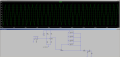
A lot of power is wasted on the emitter resistor. It seems it would be better to just put the 8 ohm resistor directly on the emitter in place of the emitter resistor.
Chris,
your base voltage may not be high enough to accomodate the entire signal.
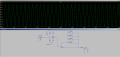
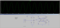
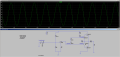
Here is an example:

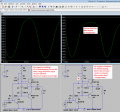
With the base voltage a couple volts above the signal imput voltage, I had no distortion with NO load.
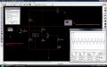
CC amp original base bias NO load.jpg

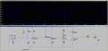
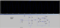
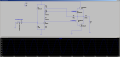
When the 8 ohm load was applied, then distortion set in.
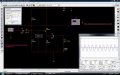
CC amp original base bias with 8 ohm load.jpg

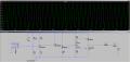
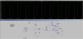
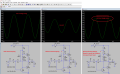
By raising the base voltage higher yet, then restored the waveform to get nondistorted symetrical output.
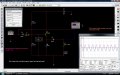
new base bias with 8 ohm load.jpg

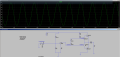
You may need to readjust base bias voltage.

Now this is all done on a computer simulator but I think it may help you with your questions.
Hope this helps.
 

Audioguru

Joined Dec 20, 2007
11,248
Sure, increase the base voltage so that the 4 ohm resistor dissipates 54.9W of heat! The CC transistor dissipates an additional 35W of heat. The total heating is 89.9W even when the amplifier has no output signal. Without any negative feedback the distortion will be fairly high.
But the output voltage swing is 9.6V peak which is 6.79V RMS which is only 5.76W into 8 ohms.
What a waste of electrical power.

The 8 ohm resistor represents an 8 ohm speaker. What happens when you have DC across a speaker? Its cone moves away from its center position. Then a signal will cause severe distortion as its coil hits the side of its magnet structure that it moved towards. Also the DC would continuously heat the speaker coil even when the speaker is not making any sounds.

With this 24V supply and 8 ohm speaker, a class-AB amplifier would produce a higher output power of about 7.6W and produce only about 1.2W of heat when it has no output signal. When its output to the speaker is 7.6W the amplifier would heat with only about 3.4W. The class-AB amplifier would probably have lots of negative feedback which cancels almost all distortion.
 

Thread Starter

cmisip

Joined Sep 23, 2017
89
I am just trying to understand the theory right now. I am not really trying to build anything.

@hobbyist
That's a great idea to try to input an AC signal directly into the amplifier output stage just to see its characteristics and then connect to the CE. I am trying to amplify a 1 volt peak ( 2volts peak to peak ) to 10 volts peak ( 20 volts peak to peak ). So far I got 8+ volts peak ( 16+ volts peak to peak ).

@Audioguru
When you proposed a push pull type class AB amplifier, do you mean as a replacement for the common emitter or common collector stage? Also what do you mean when you say the sziklai version has no negative feedback. There is a 1k resistor on the emitter of the CE stage.

This is the original multitransistor sziklai current plot on the final .0001u Ohm resistor. It is using 6.4 amperes of current maximum.

upload_2017-12-18_17-44-13.png


I redesigned it with push pull, but to achieve the voltages I needed, I still needed a CC stage. Although I managed to reduce the current at the final .0001u ohm resistor from 6.3 A to 1.1 A. The transistors will probably still burn. I am just trying to understand if this is what the exercise was for. With both of these schematic designs, the output voltage on the 8 ohm resistor is swinging at 8 volts peak ( 16 volts peak to peak ).
upload_2017-12-18_17-47-18.png. The CC stage was necessary because connecting the CE to push pull caused a degradation of the amplification. Increasing the push pull base resistors alleviated the problem in the right direction but not enough and raising them up too far caused clipping on the output voltage. This is why I decided to use the CC stage in between.

Output voltage span with push pull design at 8volts to -8 volts.
upload_2017-12-18_17-50-9.png

Output voltage span of the sziklai version also the same at 8 volts to -8 volts.

upload_2017-12-18_17-54-21.png

Thanks,
Chris
 
Last edited:

Audioguru

Joined Dec 20, 2007
11,248
Class AB is the output stage of a modern audio amplifier and opamp.
Like a modern opamp with open loop voltage gain of about 1 million (when there is no negative feedback), a modern class-AB amplifier also has a very high open loop gain so that distortion is reduced to almost nothing when plenty of negative feedback is used from the output to the inverting input. Your amplifiers do not have negative feedback from the output to an inverting input so the driver and output stage distortion are not reduced.

To produce high output current with fairly low input current, the complementary outputs are darlington or Sziklai pairs. Your circuit uses resistors to turn on the output devices and the driver transistor turns them off while carrying the current of the resistors. It seems to be backwards that a resistor produces less base current to the output devices when the current is increasing. A good amplifier circuit uses a high impedance constant current source or bootstrapping as the load for the driver transistor so that its gain is very high and linear.

A good audio website is here: http://sound.whsites.net/index2.html
Its excellent medium power amplifier (60W into 8 ohms) is its project #3A.
There are also a couple of class-A amplifiers and a constant current sink is used to replace a resistor.
 

Attachments

hobbyist

Joined Aug 10, 2008
892
I am just trying to understand the theory right now. I am not really trying to build anything.
That's what I thought, your just experimenting trying to get an understanding of what works and what doesn't work, your learning how to work with transistors from the very foundation.
I also found that increasing the supply voltage will ease the distortion as well, it's a matter of getting enough base bias to allow for the signal to ride on.

I commend you for how you are really pursuing every angle of this to see what works and how to make it work.

Because once you see how to make it work ,then it's a matter of scaling it down to real life values of voltage and current requirements for the transistors. Before you know it you'll be designing transistor amplifiers at the basic level. Which is a great start to get into this hobby.

Keep up the great work.
 
Last edited:

Thread Starter

cmisip

Joined Sep 23, 2017
89
I have been reading about bootstrapping. I think this might solve the problem with requiring a CC stage between the CE and the push pull output. It seems, a high enough bootstrap resistor would increase the input impedance of the push pull stage. This coupled with a lower CE output resistance by reducing collector and emitter resistor values of the CE should work. I am also thinking of removing the bias from the CE to the push pull stage by using a capacitor in between and have push pull work around 0 volts with a Vcc+12.5 volts and Vee at -12.5 volts. This should also even out the power usage of the push pull transistors. Right now I think the top one is using a lot of power because it is operating at a higher voltage. I will probably be able to test these ideas this weekend.

I think the reason that a bootstrap resistor can increase input impedance of a transistor is because normally, the base resistors equivalent resistance are in parallel with Vbe and emitter resistor. The bootstrap resistor would sit on top of this parallel base bias in series with it. The sum of the parallel equivalent and the bootstrap resistor would then be in parallel with Vbe resistance and emitter. Maybe.

Thanks,
Chris
 

Audioguru

Joined Dec 20, 2007
11,248
Here is a demo of bootstrapping. There is distortion because the signal level is high (but not clipping) and there is no negative feedback. The negative feedback is shorted because the impedance of the signal generator is extremely low.

Notice that the circuit with the bootstrapping capacitor connected has more than twice the gain of the circuit without bootstrapping but the bootstrapping circuit has a higher and more symmetrical output signal.
 

Attachments

Thread Starter

cmisip

Joined Sep 23, 2017
89
Thanks.

The negative feedback is shorted because the impedance of the signal generator is extremely low.
If I understand correctly, R3 is the negative feedback resistor as it goes from output into the input of Q3. Q3's input would be out of phase with the output so that would be a place to connect the output for negative feedback. The other possibility is the emitter of Q3. However, because the resistance of the sine wave source is so much smaller than R3, all the voltage drop appears on R3 so none of the output signal is impressed upon the base. Basically, where R3 meets the base of Q3, the input source impedance is so low that it cannot be pulled up or down by the feedback voltage. Is that how that works?

I played around with the bootstrap configuration and this allowed me to remove the intervening CC stage. I designed the CE to output as high a current as possible given the limit of 400 mW for 2N3904. Then the push pull stage was attached. I hope the schematic is correct. If it is correct, it seems the bootstrap resistor has a major impact on the operation of the system. If it is too low, then the Vout of the CE stage degrades. So the bootstrap is increasing input impedance of the push pull stage. I think this is happening because the input impedance of Q5 for example is equivalent to ((R5||R6)+R7))||Beta*2*Re. The Beta*2*Re is a large value that is limited by the ((R5||R6)+R7)) value. Increasing R7 would therefore increase the input impedance significantly. However, this is just at DC level. If the AC level is considered, R7 would be much bigger. The output impedance is already very small and would probably be (RC+((R5||R6)+R7)))/Beta*2. So the 8 ohm load can't pull it down. I just intuited the above conclusion on impedance values. I haven't really tested the idea on the simulator ( I did not try to connect a resistor in front with a voltage source to determine the actual impedance ). Please let me know If its wrong.

Here is the new schematic:

upload_2017-12-23_14-51-50.png

There is still some distortion at 0 volts which is magnified by lowering the bootstrap resistor value. I think all the components are within their power limits. The output is almost 20 volts peak to peak.

Thanks,
Chris
 
Last edited:

MrChips

Joined Oct 2, 2009
34,945
The little glitch at 0V is called cross-over distortion. This happens in class-B push-pull circuits. You can overvcome this by increasing the conduction current slightly, i.e. move from class-B more towards class-AB biasing.
Try adding another diode in series with D1 and D2.
 

Audioguru

Joined Dec 20, 2007
11,248
Your new circuit has crossover distortion because you have the bases of the output transistors shorted together so the diodes are doing nothing.
Your bootsrapping was odd. Try it like this but add some negative feedback:
 

Attachments

Thread Starter

cmisip

Joined Sep 23, 2017
89
You're right. I was trying to fix the distortion by tweaking and decided to put the voltages on the schematic and spotted that too. I have to analyze your schematic. I dont understand yet how to put the push pull stage on the collector of the CE. What is the R in the second diagram?

Meanwhile I came up with this updated schematic.

upload_2017-12-23_17-0-0.png

I will have to continue analyzing this schematic to see what exactly is happening.
Thanks
Chris
 

Thread Starter

cmisip

Joined Sep 23, 2017
89
I guess it really went back to the class AB without bootstrap. How would you bootstrap this and what would be the benefit? I think the output transistors are within their power limits and Vout is at expected level.

Thanks,
Chris

upload_2017-12-23_17-14-54.png
 
Last edited:

Audioguru

Joined Dec 20, 2007
11,248
Why do you continue to drive the diodes? Use Q1 to turn on the PNP driver transistor and use two series resistors to turn on the NPN driver transistor. Then the bootstrap capacitor connects from the positive wire of the output capacitor to the junction of the two series resistors so that the capacitor drives their voltage above the supply voltage and makes their current constant which makes them a fairly high impedance.

The base-emitter resistors I added to the output transistors makes sure they turn off even when they are hot.
 

Thread Starter

cmisip

Joined Sep 23, 2017
89
I tried to simulate the circuit you proposed. I must have done some mistake because the output waveform is distorted.

upload_2017-12-23_18-56-41.png
 

Audioguru

Joined Dec 20, 2007
11,248
Your amplifier has no negative feedback so its voltage gain is very high. Your input is 2V p-p and the gain is trying to make the output 100V p-p or more so the output is clipping at its maximum of 23V p-p. Simply turn down the input signal level or add some negative feedback to reduce the gain.
 

Thread Starter

cmisip

Joined Sep 23, 2017
89
I played with it a little bit and reducing the input voltage did result in an undistorted sine wave, but the amplitude was small, so I tweaked other parts to see what would happen. I did come up with this which amplifies 1 volt peak to about 10 volts peak which was my original objective:


upload_2017-12-23_22-42-50.png


As to the mechanics of this design, as far as I can tell, the push pull stage input impedance is used as a collector resistor. Because that impedance is very high, the gain would be very high as well. The dissipation of the transistors on the push pull stage have also increased to hundreds of watts if I am reading the values from LTspice correctly.

Thanks,
Chris
 

Attachments

Last edited:

Audioguru

Joined Dec 20, 2007
11,248
Without bootstrapping, the voltage gain of Q1 is (I can barely see the tiny writing) a little less than (180 + 25)/28= 7.3 times. In your new schematic, R5 and R6 should have equal values, about 100 ohms each. Then C2 should be 160uF.
 

Thread Starter

cmisip

Joined Sep 23, 2017
89
I think I recognize your design now after I moved components around. The pair of 100 ohm resistors still form the collector resistor and hence determine the gain, with two Vouts at different voltage levels sent to to the push pull stage. The problem though is the push pull transistors are above their power limits. Perhaps I need to redesign the CE stage to reduce its current output to a minimum this time.

upload_2017-12-24_7-15-2.png

Thanks,
Chris
 

Audioguru

Joined Dec 20, 2007
11,248
I never use Oriental transistors so I did not look for the ratings of the ones you used.
I simulated an amplifier with less supply voltage and less output power. It has negative feedback.
I show that when it is bootstrapped its gain is more, its maximum output level is higher and its distortion is less.
Win, win and win.
 

Attachments

Thread Starter

cmisip

Joined Sep 23, 2017
89
This has bootstrap and negative feedback. Is there anything wrong with this design? The CE is driving the diodes but that is what I see in some articles. The biasing of the push pull by base resistors allow me to control the current to the base of the push pull transistors, allowing me to put a ceiling into their power consumption. I think the theory is that a higher base bias resistor reduces the current through the diode, causing the diode voltage drop to decrease and since this is the same as Vbe, the Ib and Ic reduces also. However, I don't know how to predict the current division between the diode and the base of the transistor.

In this schematic, the sziklai transistors are dissipating under 1 watt. I don't know how to control the power usage in the schematic you proposed with two collector taps 1.4 volts apart.

Is there a best practice approach with bootstrapping and negative feedback?
upload_2017-12-25_16-38-34.png

Thanks,
Chris
 
Last edited:
Top