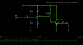
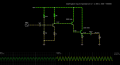
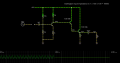
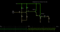
Common emitter npn Ib and Ic

Audioguru

Joined Dec 20, 2007
11,248
This is a horrible way to bias a transistor.

I disagree that you "assume" a beta when designing a transistor circuit. A transistor has a wide range of beta, this one assumed to have a beta of 100 might have an actual beta of 300 then this simple one resistor bias method will not work and the emitter voltage and current will be much higher and the little transistor will try to dissipate about 1.7W and burn up.

Instead the base should be biased with a voltage (not a current) set with a two-resistors voltage divider.
 

hobbyist

Joined Aug 10, 2008
892
The above solidifies the idea that looking from the base towards the emitter, the emitter resistor looks like it is RE * Beta.
You'r getting a good hands on experiance in learning this, I could tell you that "B*RE" needs to be considered when determining Zin of a stage, but it's not until you do what you'r doing, picking the amp apart piece by piece and analysing until you learn it for yourself the how's and why's of the theories presented., I commend you on your pursuit of learning this. Great job.

QUESTION2: Where did I make a mistake on the power calculation?
You'r power calculation isn't wrong, however, I'm just guessing here, to calculate power diss. of this as an amplifier, you need to consider it under and AC signal. Your power cal. is being done using DC analysis.
You would need to use AC analysis to determine power Dissipation I think.

QUESTION3: Do I need to worry about the previous CC stage's output impedance? It's a CC stage so it should be low. Do I worry about matching the previous CC output impedance with the following CC input impedance?
I would suggest that would be a good design change, as well as an exercise in going further on your own, now that your understanding this much better now. You may have to recalculate values along the way, but that's what this is all about, learning how to bias the transistor stage for any reasonable voltage and currents you desire.

Thanks for reporting back your observations, I see your really getting a good understanding of this from the very basic level.
 

Thread Starter

cmisip

Joined Sep 23, 2017
89
@hobbyist
I think I was able to follow your calculations. The CC stages were designed to deliver 4 volts to the speaker. This would be the voltage across the emitter resistor of Q1. The base voltage that was set for Q2 considered the .7 volts drop that would be incurred when the voltage was sent to Q1 and passed the base to its emitter. That's why that base voltage calculation included two .7 volts.

How did you figure that the speaker would only draw 45.6 mA? My simulation shows that it is pulling 110.2 mA and that it is pulling the CC Vout to .8 Volts.

Ruminations in the shower reveal these things:

1. I think that perhaps it is not necessary to worry about impedance matching between CC stages. This is because the CC to CC connection is an ideal connection in the sense that the previous CC would have low impedance at output and the following CC stage will have high impedance. This means that the second CC stage could not draw too much current from the first CC stage. Even if it did, the first CC stage has low output resistance that its Vout will not sag regardless. The impedance matching must happen between the CE and the first CC stage and between the last CC stage and the speaker. If this were true, then what would be output impedance of the CC stage before the speaker. Output impedance formula state that it is Rsource/Beta+1. In this case then would Rsource be the CE stage RC?

2. The other thing I was thinking about is that this an amplifier design so therefore, the operational properties has to be what we would see if we have an actual AC signal riding the bias. This would short out all the capacitors and present input and output impedances that would be different from those that were calculated when there was no AC. Shouldn't the impedances be calculated with the capacitors shorted and matching performed on those values instead of just with the DC bias voltages and currents?

3. The other thing I was thinking about is that an entire amplifier stage could be reduced to a single resistor with voltage and current. The texts I read about this seem to suggest that amplifier stages that are connected together form a voltage divider between the preceeding and succeeding stages. This would suggest then that the best case scenario for impedance matching is a reduction of Vout by 1/2. Because if a resistor has current and voltage and we consider one end of the resistor as Vout, If I connect a wire to Vout to ground ( attach a resistor that has very low resistance ), then I would have pulled the voltage all the way to zero because I pulled all the current. Conversely, if there is nothing connecting that Vout to ground ( condition of infinite resistance between Vout and ground ), then Vout remains the same as I have not pulled away any current. If this is true, impedance matching would cause the speaker to pull the 4 volts output of the CC Q1 stage to 2 volts if they are properly matched. How much the speaker pulls down Vout of Q1 CC could also lead to discovering Q1 CC's output impedance. With the CE <-> CC connection, we could expect the same Vout reduction by 1/2. So this concept is a bit confusing to me at this time. It seems if we wish to preserve Vout from each stage to the next, we ought to shoot for the preceeding stage to have low output impedance and the succeeding stage to have high input impedance and not a matched impedance.

The shower ruminations end here.

P.S. I posted this before realizing that there were already two previous posts after my last post last night. I will have to read the two previous posts and their implications after dinner.

Thanks,
Chris
 

hobbyist

Joined Aug 10, 2008
892
Hi Chris,
Ok, I have to really go over what you wrote and read it carefully to be able to answer most of the concerns, however, these exercises were mainly shared to help you get a feel for biasing a transistor for any reasonable current and voltage, wether it is an amplifier, or a current source or voltage reference.

I was trying to show, how to deternine the amount of current a transistor would take when it is parrallel with a DC load, such as Q2 being part of the bias network for Q1 and Q3 feeding bias voltage for Q2 ect...

Then I introduced making it into an AC amplifier, just to see how well it would turn out.
To my surprise the actual circuit build on my breadboard proved to be a good working small sig. amp, to drive my stereo spkr, 20ft. away in the next room to a audio level about as loud as the source (IPAD), using a spkr. for the input device and a 9 volt battery.. So it is a workable design that could encourage youi to play around with it and improve on it.

The CC stages were designed to deliver 4 volts to the speaker.
No, the output voltage pk-pk I was designing for around 360mV across the 8 ohm spkr. (AC coupling)
Another thing to consider AC analysis needs to be done on a spkr load, because the 8 ohms is referring to total impedance, not just physical resistance of the windings.

The reason you were thinking 4V output across the load was because of the 4V at the emitter.
However the load is actually capacitive (AC) coupled to the emitter leg. So we have an initial value of 0V, then a pk volt. ~180mV if it could be realized.

Getting to your questions on Zout of CC, this is where you will need to do some research on,Quote"Output impedance formula state that it is Rsource/Beta+1"(looks like you've been doing some studying on this), because the Zout of a CC stage is complicated with more than just the load and emitter resistance, there is also the source impedance to consider and such, too much to get involved with right now.

Quote: "In this case then would Rsource be the CE stage RC?"
As per your question without doing an analysis on this, I would say yes the CE collector resistor would be the Zout of the source to the CC input. Just guessing at the moment.

However If you build (or simulate ) the entire circuit I drew up, then experiment changing resistor values, I think you will get a good hands on learning experiance of what works and doesn't work, and why.

Please continue to report back your findings, because, The questions you are bringing up are helping me to delve more into this design work as well.

I'm digging more into my course material to try to find the answers to your questions, which is a good learning exercise for me as well.

As I said I will try to answer your questins on the above post on my next post.
 
Last edited:

Thread Starter

cmisip

Joined Sep 23, 2017
89
No, the output voltage pk-pk I was designing for around 360mV across the 8 ohm spkr. (AC coupling)
Another thing to consider AC analysis needs to be done on a spkr load, because the 8 ohms is referring to total impedance, not just physical resistance of the windings.
You are right. The capacitor takes out the bias voltage leaving the AC voltage on the 8 ohm speaker. i also just realized that the design schematic you posted looks very much like a Darlington Pair.

I thought I'd whip up a quick simulation testing the idea of matching input impedances. The theory is that if I match the output of the CE stage to the input of the CC stage, then the Vout will be reduced by half.

In the next screenshot, the Vout of the CE is clearly shown as 10.3 volts. There is no AC current. I chose the emitter resistor to be 1 ohm so I can multiply to 10k with the hfe of the transistors. 1 ohm emitter resistor selected also because it makes the Vout of the Darlington pair resistant to voltage sag when connected to the 8 ohm speaker. This is because a high (8 ohm) impedance is matched to a low (1 ohm ) impedance. With the capacitor to the 8 ohm impedance shorted, the parallel resistance does not change much from the 1 ohm value. In all these simulations, the input impedance of the darlington pair is computed as hfe x hfe x RE. The output impedance is RC / hfe /hfe. For the 100 hfe, this would be 1 ohm. For the 300 hfe, this would be .111 ohms. In both cases, assuming the math is correct, the output impedance of the Darlngton pair is much smaller than the 8 ohm impedance of the speaker. This is really a simplification of the long form input and output impedance but should be good enough for approximation.

upload_2017-12-11_22-53-15.png

In the next screenshot, the transistors of the Darlington pair are set to have an hfe of 300 each. So the input impedance of the darlington pair considering the 1 ohm emitter resistor is 90000. Due to the much higher input impedance, we don't expect the Vout of the CE stage to sag very much. It shows that it is staying at around 9.4 volts.

upload_2017-12-11_22-49-36.png

With the AC signal connected, the output voltage has increased from 20 mv to 64.26 mv peak voltage.

upload_2017-12-11_22-48-37.png

If the hfe of the transistors is changed to 100 and the AC signal disconnected, the CE output impedance matches the input impedance of the darlington pair. The result is a ~50% reduction in Vout which is now at 5.9 volts.

upload_2017-12-11_22-52-5.png

With the AC signal connected, the output voltage has increased from 20 mv to 35.78 peak voltage. Ignore the text label below. It should have read Darlington input impedance is 1 x 100 x 100 = 10000.

upload_2017-12-11_22-56-37.png

The simulation can be recreated by importing this text into the falstad circuit simulator.

$ 1 0.000005 18.278915558614752 60 15 53
w 80 16 176 16 0
r 80 16 80 176 0 110000
r 80 176 80 320 0 10000
t 80 176 176 176 0 1 -4.468107884463787 0.5943481843397954 100
w 80 320 176 320 0
g 80 320 80 352 0
R 80 16 -16 16 0 0 40 20 0 0 0.5
r 176 16 176 160 0 10000
r 176 192 176 320 0 1000
c 80 176 0 176 0 0.0000049999999999999996 1.5772785548384245
R 0 176 -80 176 0 1 80 0.02 0 0 0.5
t 304 160 352 160 0 1 -13.973908020790866 0.6936347202022768 100
w 352 176 352 240 0
w 352 240 384 240 2
t 384 240 432 240 0 1 -14.667542740993142 0.8130048123704432 100
w 176 160 240 160 2
w 176 16 352 16 0
w 352 16 352 144 0
w 352 16 432 16 0
w 432 32 432 224 0
w 432 32 432 16 0
g 432 304 432 352 0
r 432 256 432 304 0 1
w 544 256 592 256 2
r 592 256 592 320 0 8
g 592 320 592 352 0
c 480 256 544 256 0 0.00009999999999999999 4.498585003562275
w 432 256 480 256 2
x 282 129 342 132 4 18 100\shfe
x 443 207 503 210 4 18 100\shfe
x 285 -13 561 -10 4 18 Displaying\sVout\sof\sCE\sat\s10.3\svolts
w 240 160 304 160 0
o 10 64 0 4098 0.078125 0.00009765625 0 2 10 3
o 24 64 0 4099 0.15625 0.0125 1 2 24 3

I will continue my studies on this. This is really interesting.

Thanks,
Chris
 

Attachments

Thread Starter

cmisip

Joined Sep 23, 2017
89
An additional observation is that the same voltage sag is causing the peak to peak voltage span to reduce at each stage. If the hfe is set at 100, then then peak to peak voltage is .2 volts span . If the hfe is set at 300 then the peak to peak is .34 volts span. This is measured at the collector of the CE and the emitter of both CC's. So impedance matching reduces the gain.

Thanks,
Chris
 

Thread Starter

cmisip

Joined Sep 23, 2017
89
Just playing around with the input and output impedances. I tried to see what each stage looked like to the other. It seems Q3 sees Q2 and everything behind it as a 11.5k ohm resister in series with itself ( with its own output impedance as 10k ) with a voltage source of 10.3 volts between them and GND. Also, Q1 sees Q2 as a 101 ohm resistor in series with itself ( with its own input impedance as 100 ohms ) with a voltage source of 10.3 volts between them and GND. I added the diodes for the voltage drops of the Vbe junctions.

upload_2017-12-12_15-56-35.png

I am still not sure how I would predict the current consumption of the 8 ohm load but it seems that If I keep the resistance of the 8 ohm load much higher than the Q1 CC output impedance, I needn't worry because the load can't draw too much current. The output impedance of Q1 CC facing the 8 ohm load would be 10k/100/100 = 1. It seems that it should also be pointed out that with a higher hfe, the emitter resistor on Q1 CC would actually look a lot less than 1 ohm. In theory therefore, the 8 ohm resistor would be in effect in series with a very low value resistor even though the diagram shows that they are parallel.

The current through the base of Q2 would be computed as (10.3 -.7 -.7) / (100 + 101) = 44.23 mA. I think that is correct. This would control the current through Q1's collector. So it would be possible to change this base current and hence the power dissipation of Q1 by manipulating the value of the Q1 emitter resistor since it is in series with the output impedance of Q2. Just need to remember that when the calculation is done on the base side of Q1, the emitter resistor is actually Beta * emitter_resistor.

I think that is what is happening. Please provide any corrections in case you spot errors.

Thanks,
Chris
 

Attachments

hobbyist

Joined Aug 10, 2008
892
Hi Chris,

Just to let you know I'm following along with your posts, I'm working on some more practice exercises to help enhance what you are learning and posting on your thread.

When I get something put together that can be of benefit to what your learning and the questions your asking, I'll post it.
 

hobbyist

Joined Aug 10, 2008
892
Ok I'm trying to keep up here, lets go back to post #85, where you were changing the beta's of the transistors (darlignton pair) and bias voltages were changing significantly.

First of all so no one takes your circuit the wrong way, we need to acknowledge, that the VCC and the one ohm resistor, is only for simulating a concept chris is working on. This is not a circuit design but he is experimenting with worse case senarios, to prove some doubts he's finding.

we ought to shoot for the preceeding stage to have low output impedance and the succeeding stage to have high input impedance and not a matched impedance.
When I used the term impedance matching, not referring to equal impedances, but rather the matching of signal flow impedance, meaning impedance from one stage to the next as the signal is concerned, which allows least amount of signal loss and ideally no distortion, if possible.

Ok now analysing your circuit, (post #85) the beta of a transistor has to do with current (IC / IB) therefore base current is the cause of amplification in the transistor, but also the cause of source loading, which fights against the signal coming in.

So if your darl.pr. has a very high beta, then little current is taken by the base, so the voltage divider formed by the transistor and its collector resistor is able to keep a stable voltage at the output.

When you changed the beta of the pair, to a much lower value your output voltage dropped considerably, due to base current loading the divider.

To remedy this, redesign the CE stage so that the current flowing through the transistor has around 10 times more than the base current into the darlignton pair.

In order to do this, choose a very low value for Beta at the darlington pair, in calcualting the emitter current for the CE stage.

For instance if you used a value of 20 for the beta of both darlignton transistors.

1/2VCC across 1 ohm would be (10V / 1 ) = 10A current. for the emitter current into the output transistor.
now divide that current by 2 beta's of (20) to get 400, therefor (10A / 400) = 25mA, for the base current of the input transistor of the darl. pair.

Now calculate the current the CE stage will take in order to produce a voltage at it's collector of 1/2VCC.

This current needs to be at the very least 10 times greater than the 25mA of base current of the darl.pr.
That would be 250mA of IE for the CE stage.

So now to put 10V at the collector, would be (10V / 250mA) =~ 43 ohms for RC
now arbitrarily choose a value of emitter voltage, ex. 3V so (3V / 250mA) = 12 ohms for RE

Now make the base pull down resistor in the divider be 20 times RE or around 240 ohms.
Now pull up calculates out to be around 1K ohms.

Now this is an impossible design with regular small signal transistors, however using your simulator you can work with this.

I have on my IPAD "ICIRCUIT" it allows me to simulate these on the fly real quick, however it doesn't use transistor models but it allows concepts to be worked out somewhat.

Therefor I built the circuit with the values I showed above and started with the beta's of the darlignton pair as Beta = 200 for each transistor.
the output voltage across the 1 ohm emitter resistor was (8.85V)

Then changed the beta's to (20) for each transistor in the pair, and ouput across the 1 ohms showed (8.03V)

So very little change from a beta of 200 to 20. (8.85- 8.03V) = 820mV change.

Now for design sake, I chose to put 1/2VCC at the collector of CE stage, this is good when AC coupling, however for this DC coupling, I should have calculated the voltage at the base of the darl. pair, and considered the current needed to maintain its output voltage ect...

So just be aware that this was not to design for a specific DC output voltage, but just to demonstrate Beta changes and how to swamp its influence as much as possible.


In conclusion you can see that by biasing your base divider with a much greater amount of current than the base current, allows the base voltage to remain stable due to low base current loading, thereby keeping emitter voltage and thus emitter current stable throughout the range of beta changes.

When designing transistor stages for biasing always use the lowest value of beta given that way you are able to make accomadations for the whole variety of transistor substitutes if needed.

I'll continue with your new posts after I catch up reading them, to answer any questions you have in them.
 
Last edited:

Audioguru

Joined Dec 20, 2007
11,248
Didn't you calculate that the poor output transistor is heating with (20V - 4.4V)/4.4A= 68.6W but its output power into the 8 ohm speaker is only 1.9W just before clipping. The poor output transistor heats with 68.6W even when there is no output signal.
 

Thread Starter

cmisip

Joined Sep 23, 2017
89
To all of you especially hobbyist and Audioguru, thanks for taking the time to teach me and thank you for sticking around. I've learned a lot here and there are more to learn.

@Audioguru
I was aware of the 4.4 A but did not check the power consumption to see if it is within real world limits. The goal of the simulation was just to discover the relationships of input and output impedances, signal attenuation and mechanics of current and voltage calculations using input and output impedances as opposed to actual real resistors with easily calculable values. I couldn't do it in LTSpice because I don't know how to come up with a custom transistor with a custom beta. In falstad, I could change the beta to 1000 and it would accept the change.

To remedy this, redesign the CE stage so that the current flowing through the transistor has around 10 times more than the base current into the darlignton pair.
I was thinking around the same lines. The alternative solution is to come up with a higher input impedance on the CC stage so that it is 1:10 ratio of output CE to input CC impedance. But I was also thinking that I could use the existing bias at the collector as base voltage for the CC stage. That is to plan for a lower Q point for the CE stage, at the same time present a huge 1:10 difference in impedances so the lower Q point collector voltage gets preserved when the CC stage is connected. Probably a combination of both approaches is necessary so the component values fall within real world limits. I am finding that there is no voltage span contraction with the Vbe drops. The voltage span contraction along with Vout reduction ( which pulls the Qpoint towards cutoff ) only happens where the CE meets the CC when there is excessive current draw by the CC stage.

I will try to simulate the possible solutions but this time I will also try to keep an eye on power consumption.

Thanks,
Chris
 

hobbyist

Joined Aug 10, 2008
892
but this time I will also try to keep an eye on power consumption.
Let's go back to your original post with the CC amp design.

Your under the impression you need to match the impedance of the emitter resistor to the 8 ohm load.
This is where you are getting very unusual values of currents and voltages power consumption.

First you'r CC amp is not amplifying voltage, it's supplying current to a low impedance load, the emitter resistor is not the CC amps output impedance to match to the 8 ohm load, that's why your 1 ohm resistor is giving a lot of problems with input impedances to your output stage and such...

I'll write up the design steps (from my course material) of designing a CC amp and post it here and you can start with common values of currents and supply volotages that will actually be useful for a real world design.

That way you can get a better understanding of how to approach these design criterias, otherwise you woud be running in circles trying to manage power consumption and such.
 

hobbyist

Joined Aug 10, 2008
892
Lets go back to square one, and get real parameters to work with so this thread doesn't get way out of proportion.

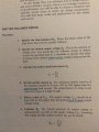
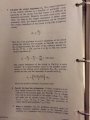
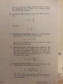
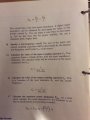
Here are pics. I took of my course material from NRI, we'll go over the steps to design a basic CC amp to drive an 8 ohm spkr, within reasonable power consumption.


CC 1.jpg CC 2.jpg cc3.jpg cc 4.jpg


First of all let's get all of our parameters set up, from data sheets ect..
A common 2n3904 transistor is easy to aquire so use that for the design work.
Max Pdiss =~650mW.
use a common easy to get 1/4wt. resistors. so Pdiss= 250mW

Doing a audio check across a 8 ohm transistor radio size spkr. 300mV is plenty of output voltage to develop across it for an audi tone to be heard.
Now this is a 1Wt. spkr.

Lastly design this to work off a 9V battery partly depleted, so VCC can be designed for 7V, worse case:

Set up design equations:

P=(E x I) ....P=( I^2 x R)

Here is where circuit design becomes an art, you have to use your available parameters to calculate for the given steps of design.

How much power do I want for the transistor to use up. I'm choosing 400mW just to see if the transistor can handle it ok, as well as have enough power to drive this very low impedance load.

So looking at the spkr parameters max current { Imaxspkr. = (P /R)^1/2 } "square root of (P / R)"
sqrt. (1 / 8 ) = 353mA. (At his point I'm not sure if the spkr. ratings for power is pk. or pk-pk.)
However for this design exercise it won't matter as were using a small output voltage to drive it with.

looking at step 1 in the pic 1.
RL=8ohms.
VL = 300mV pk-pk.
IL = ~38mA pk-pk.

step 4: choose 20% higher.
IE=(1.2 x IL) =~46mA.

Steps 5-6: Vcc is chosen at 7V and (RE = VCC / 2IE)
RE = (7 / 92mA) =~75ohms

skip steps 7-9 that is showing dc coupling of a CE stage to it.

This is a design for just the CC amp alone driving a low impedance.

steps 10-13. choose a low value of beta (make it 50), and make the divider current 10 times larger.
IB = (46mA / 50) =~920uA
ID =~9.2mA
RA=RB (VCC / 2ID) =~390ohms.

Build it and tweek it to get around (1/2VCC - Vbe) across the RE resistor.

Don't worry about steps 14-17 for right now, just use large 100uF caps for input and output:
You can study those steps on your own at your leisure.

Then apply a signal around the 300mV range to check for no distorted output across the 8 ohm load, remember to cap. couple the 8 ohm load. This is designed for an AC load on its output.

Then increase the input signal until you get distortion, this is tghe max input you can apply to this stage.
Then from there we'll work back to the input coupling stages together as before to raise the Zin of this stage and so on.

This excersise will get you familiar with designing real circuits by working within parameters, as all circuit designs requires.

The actual dynamic test results are in the next post.
 
Last edited:

hobbyist

Joined Aug 10, 2008
892
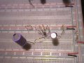
Breadboarded circuit

SUNP0001.JPG

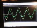
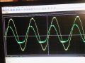
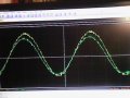
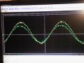
Ok using 75ohms for RE gives bottom clipping with an input of ~1.3V and CC ouput around 684mV.


SUNP0002.JPG


When I checked the DC bias on the RE it was low (2.85V) , due to the RA and RB value dividing the supply in half, leaving the VE less by a Vbe drop.

Therefor at these low output voltages it's a good idea to design for as close to possible a 1/2VCC across RE.

Therefore,
redesign values for the base divider, changing the pull up resitor to 270 ohms made the VRE now be ~3.4V

so here is what the waveform looks like before the change

SUNP0004.JPG

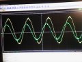
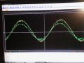
and after the change of resistor value, swapped out one resistor (pull up resistor from 390 to 270) ohms.

SUNP0005.JPG

it is the same input signal!

So that shows why its important to test your work at each stage of the design I calculated the value change, however it could of been just as easy to tweek the resistor values imperically watching the VRE on a voltmeter.
Now all that was on a test freq. 200HZ.

Using a test frq of 1Khz.:
and 100uf coupling caps gives:

Vin pk-pk =~922mV
Vout pk-pk across an 8 ohm resistor load =~722mV

SUNP0006.JPG

SUNP0007.JPG

Now here is something to note:
Removing the 8 ohm dummy load (simple 1/4wt. 8.2 ohm resitor),
and hooking up the spkr itself, gave audible audio output, here is the waveform:

SUNP0008.JPG

SUNP0009.JPG

As you see the waveform is better with the spkr, due to the fact that the dummy 8 ohm resistor load was given 8.2 ohms of resistance to the circuit under any freq.

The spkr is inductive as well as resistive, this is impedance, and the signal output was larger for the ratio of input to output, due to the XL of the spkr raising the impedance higher than the resistor alone.

Also the output voltage is always smaller than the input due to the Vbe drop, so a CC has a gain of Av<1 but has large current gain to drive a low impedance load.

Lets do one more test if we raise the voltage to 9V fresh battery how will the circuit perform.
SUNP0010.JPG

SUNP0011.JPG

pretty stable input to output waveform ratio and no distortion.

These 2 lessons in CC design should give you some basic background to work from.


Practice designing this for different load impedances until you'r ready to couple this to some preamps stages.
 
Last edited:

Thread Starter

cmisip

Joined Sep 23, 2017
89
@hobbyist
Thanks a lot for this. It will take me a while to digest all this information. I have gotten slightly busy at the moment but I will pour over these as time permits.

My goal is to see if I can design an amplifier with the information so far learned. I will continue to play with the simulator to solidify certain concepts and to check what happens when I modify parameters.

I just found out that the loading issue occurs as well at the junction of R1 and R2 with the base of the transistor of a CE stage. If RE is lower than R2, it tends to pull the voltage at the junction down increasing the current draw into the base and pushing the transistor into saturation ( past calculated values of base current) . It seems this can be avoided by keeping RE >> R2, or perhaps RE >> R1||R2 because R1||R2 potential divider can be effectively equal to one resistor that provides base bias. I ran into this issue trying to design the CE stage for maximum current which meant the collector /emitter side resistances needed to be small. However, there is the conflicting problem of the input impedance of the CE amplifer being effectively R1||R2||Beta*(Re+re). If R1|| R2 is small relative to RE, then it follows that they will pull the input impedance down as they are all in parallel to Beta*RE. So increasing the CE stage current has the unfortunate disadvantage of decreasing its input impedance. A compromise needs to happen and rules of thumbs have been suggested where I always see 1:10 as a recommendation. This ratio seems to be recommended for impedances and currents.

I will continue my studies.

I have run into this information:

Line/Headphone Output

The line/headphone output is automatically selected for audio output if no external device is detected at the S/PDIF optical digital output port. The line/headphone output supports a stereo data stream at bit depths of 16, 20, or 24 bits per sample and at sample rates of 44.1 kHz, 48 kHz, or 96 kHz. The line/headphone output volume can be adjusted from 0.0 dB to -95.25 dB.

During playback of a 1 kHz, full-scale sine wave (44.1 kHz output sample rate, 24-bit sample depth, 100 kΩ load, unless otherwise specified) the audio line output has the following nominal specifications:

Jack type: 3.5 mm stereo
Maximum output voltage: 2 VRMS (+8.24 dBu)
Output impedance: < 24 Ω
Frequency response: 20 Hz to 20 kHz, +0.5 dB/-3 dB
Signal-to-noise ratio (SNR): > 90 dB
Total harmonic distortion + noise (THD+N): < -80 dB (0.01%)
Channel separation: > 75 dB

Note: For best results, equipment plugged into the line/headphone output jack should not connect the audio ground to other grounds, such as the chassis or “green-wire” ground.

A couple of quick questions.
1. What is the input voltage peak to peak in this case?
2. In this case is 240 ohms input impedance sufficient for a CE stage to match with a PC line out?
3. What magnitude of gain needs to be realized to amplify the line out signals to drive a 8 ohm or 16 ohm speaker?
4. What would be a reasonable power level that needs to be delivered to a speaker. I realize that this last question depends on the speaker. However, I just would like to have a practical target for the simulation.

Thanks,
Chris
 

hobbyist

Joined Aug 10, 2008
892
A couple of quick questions.
1. What is the input voltage peak to peak in this case?
2. In this case is 240 ohms input impedance sufficient for a CE stage to match with a PC line out?
3. What magnitude of gain needs to be realized to amplify the line out signals to drive a 8 ohm or 16 ohm speaker?
4. What would be a reasonable power level that needs to be delivered to a speaker. I realize that this last question depends on the speaker. However, I just would like to have a practical target for the simulation.
Hi Chris,

The topic above is beyond the scope of my understanding, this would probably be more in line what audioguru could help you with.

I can help you design a basic audio amplifier picking up from where I left off at (post #93 and #94).
 

Audioguru

Joined Dec 20, 2007
11,248
A couple of quick questions.
1. Maximum output voltage: 2 VRMS. What is the input voltage peak to peak in this case?
The gain of the circuit determines the input voltage. The 2VRMS output has a peak voltage of 2V times 1.414= 2.828V then it is 5.656V p-p.

2. Output impedance: < 24 Ω. In this case is 240 ohms input impedance sufficient for a CE stage to match with a PC line out?
It will work but why is the input impedance so low?

3. What magnitude of gain needs to be realized to amplify the line out signals to drive a 8 ohm or 16 ohm speaker?
You forgot to say the amount of output power. 0.1W into 8 ohms is 0.9VRMS then the gain (loss) is 0.9V/2V= 0.45.
The voltage of 100WRMS into 8 ohms is 28VRMS. Then the gain is 28V/2V= 14.

4. What would be a reasonable power level that needs to be delivered to a speaker. I realize that this last question depends on the speaker. However, I just would like to have a practical target for the simulation.
Depends on what you like and how you do it. Many people have a sound system in their home that is 70WRMS into 8 ohms per channel like mine in my living room. My clock radio in my bedroom produces about 1WRMS into 8 ohms and I use both frequently.
 

Thread Starter

cmisip

Joined Sep 23, 2017
89
It will work but why is the input impedance so low?
I was going with hobbyist's line of thinking with regards to the problem of CE output sagging when connected to the CC stage. If I keep the CE Ic and Ie high compared to the current draw of the CC stage, then the CC stage can't pull down the CE Vout. This meant keeping the resistances on the collector emitter side low and since the input impedance is the equivalent resistance of R1||R2||B*RE, B*RE will probably be the lowest of the three and dictate the input impedance. I needed to know what was the minimum required input impedance to match with the PC line out.

I've been thinking about this a bit. What I wasn't sure about was how to predict the current division between the load and the emitter resistor in the CC stage where it interfaced with the speaker. What if multiple speakers were wired in parallel, then the resistance would reduce. It seems that a good amplifier would need to be able to drive enough currents to support different configurations. This put impedance matching at the CC stage out the window because we now have a range of speaker impedances that we need to design for. Not that impedance matching at the CC to speaker stage was that practical a solution because the CC stage's output impedance is very hard to pin down to a specific value. It is easier to make it as low as possible.

I think setting up the IE to be 20% IL is probably considered best practice. However, the load will pull whatever current it needs at whatever happens to be the Vout. There is no way to saturate the CC stage and current division at the emitter between load and emitter resistor is made more complicated by negative feedback. As soon as the load tries to pull down the Vout, the base current increases, increasing Ic and Ie, which in turn restores Vout to its original value. If Ie and Ic are too high, then the transistor burns out because we can't turn it off when the Ic is too high. The maximum current required by the load + 20% will be the ceiling for IE/IC I think for power calculations. This CC stage will in turn require more base current from the previous CC stage as it tries to meet the load current requirements. There again at the CC to CC connection where the previous CC sees the next CC as a resistor, it will try to maintain the Vout and pull more base current from the CE stage.

We can look at this from two perspectives. Due to the load, the darlington pair is drawing more current from the CE stage hence pulls down the Vout at the CE collector which in turn puts the Darlington Vin lower. The other perspective is that the load pulls the effective resistance of the Darlington pair down such that voltage division pulls CE collector voltage down.

The reason why the amplifier's Vout might fall then is because of the drop at the CE to CC connection reducing the Vin to CC. The CC will work with whatever Vin it is given and will maintain that ( less the Vbe drops) or burn out as it tries to meet the current requirements of the load.

Please let me know If there is anything wrong with this analysis.

Thanks,
Chris
 

Audioguru

Joined Dec 20, 2007
11,248
The Vbe of a transistor increases when its collector-emitter current increases. In an audio amplifier without negative feedback this causes compression distortion (odd harmonics) if the amplifier is push-pull and causes asymmetric distortion (even harmonics) in your single transistor output. Negative feedback will increase the gain and base current so that the distortion is reduced.

You keep talking about "matching" impedances when an old vacuum tubes amplifier was used. Modern amplifiers have a low impedance feeding a high impedance so that voltage division is small.
Modern amplifiers do not burn out when they have current limiting.
 

Thread Starter

cmisip

Joined Sep 23, 2017
89
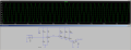
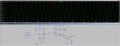
What is wrong with this schematic? I am trying to see if I can amplify a 1 volt peak ( 2 volts peak to peak AC ) to 10 volts ( 20 volts peak to peak ). I used a three stage CC to reduce the CC stage impedance so i dont load the CE. That seems to have worked and the bias is preserved when the CC stage is connected. Three Vbe drops later, the bias is still at the correct level. The amplification survives up to the final capacitor as the graph shows. However, when I connect the 8 ohm load, it pulls the voltage down.

upload_2017-12-16_15-58-41.png

upload_2017-12-16_16-4-52.png

Is there just not enough current?

Thanks,
Chris
 
Top