Common emitter npn Ib and Ic

Audioguru

Joined Dec 20, 2007
11,248
My gosh, the chicken and the egg they arrive at the same time! Could you provide a general explanation.
In post #179 I explained: "When the 25VDC power supply is turned on some current goes through R3 and R7 to turn on Q5 which provides current to R6 that turns on Q1. The DC negative feedback stabilizes the output at the correct DC voltage."
 

hobbyist

Joined Aug 10, 2008
892
The feedback from the output of the CC stage to the input of the CC stage
Chris, correct me if I'm wrong , I don't think you have CC stages anymore, Q3 and Q4 are driving R9 on there collectors, and Q5 and Q6 are driving the bases of Q4 and Q3 on there collectors.
Q5 and Q6 are connected to the load, but there not driving the load any more since Q3 and Q4 are in the output branch now.
 

Thread Starter

cmisip

Joined Sep 23, 2017
89
@hobbyist
Sorry, that quote was a typo. I meant negative feedback from the output of the CC stage to the input of the CE stage ( I think that is called global negative feedback ) as differentiated from emitter degeneration or collector to base feedback.

I do still think that the push pull stage even in the latest schematic without the CE base bias resistors, is still a CC stacked on top of another CC ( They operate on different voltage ranges, one from VCC to VCC/2 and the other from VCC/2 to GND. That way when they add up at the output, they are in proper position relative to each other and form a full sine wave which is centered at VCC/2. The capacitor will then center to GND by removing the DC bias). They don't operate concurrently except at the crossover where they might both be turned on but one turns off as the voltage swings in the positive direction and vice versa. If you follow the arrows of the emitters, you can see that the currents add up for Q4 and Q5 and for Q6 and Q3 which are series connected. Each pair can be treated as one transistor with the hfe's multiplied. For that matter, any number of parallel connected transistors could be treated as one big transistor with hfe multiplied by the number of transistors. For analysis, I just considered one half of the push pull stage to be OFF. In this case though, the emitter resistor of the CC stage is the speaker impedance. Earlier I noted that a lot of power was being dissipated in the emitter resistor of the CC stage when there is a parallel load connected to it. In this case, the power is being used at the speaker. Nobody here has confirmed or denied this assumption though. I am sure my analysis is chock full of holes as well.

This configuration that I am using is a sziklai specifically to avoid the second Vbe drop of a Darlington. I was contemplating adding another pair of transistors at the shoulder to increase input impedance without having to add emitter resistors ( as I thought the input impedance of the CC stage was too low and that is why I was not seeing the 1000 gain. Raising the output impedance to 800 seems to confirm the impedance issue as that allowed the 1000 gain to manifest. ) but Audioguru's solution is much better and with fewer components.

What I am trying to understand right now is how the latest schematic is able to work without the base bias resistors to the CE stage. I think its because the DC bias of the output ( in addition to the output AC) is carried over to the input ( degraded by the feedback resistor ). Then the output AC (degraded by the feedback resistor also) riding the bias is subtracted from the input AC ( because they are 180 degrees out of phase ). The DC bias is preserved and is keeping Q1 in the ON state and the summated AC input is riding at the top. I think this is what Audioguru meant ( or it is just another fantastical story I came up with ) when he wrote :

In post #179 I explained: "When the 25VDC power supply is turned on some current goes through R3 and R7 to turn on Q5 which provides current to R6 that turns on Q1
The concept of input and output impedance takes on a new twist in the face of bootstrapping and global negative feedback.

I'll be reading more about this.

Thanks,
Chris
 
Last edited:

Thread Starter

cmisip

Joined Sep 23, 2017
89
I did some more research. Please let me know if any of the following analysis are wrong.

It seems that global negative feedback ( feedback from output stage to input stage when there are multiple stages in the amplifier ), is applied usually at either the input stage base or input stage emitter.

If applied at the input stage base, since the output is 180 degree out of phase with the input, then the feedback subtracts from the input voltage amplitude. This results in a smaller value for Ib.

If applied at the input stage emitter, the output is in phase with the emitter signal ( so in phase or out of phase DOES NOT define wether feedback is negative or positive, it is the effect that defines ) and hence adds to the emitter voltage amplitude. The effect is that the emitter voltage is more positive which reduces Vbe, reducing Ib.

Both the above type of negative feedback reduce Ib and so increases the apparent resistance of the input stage to the input signal.

On the output side ( the final stage ) where the feedback is coming from, the effect is to reduce the output impedance wether the feedback is tapped from the collector or the emitter. This is because if there is any effect that happens to pull down the final stage's Vout, this will reduce the feedback voltage, which will increase the input stage Ib, therefore raising the final stage's Vout again.

One other effect that could pull down the final stage's Vout is Beta variations of the transistors in that stage. It would seem that this effect will be reduced by global negative feedback as decreased gain for example from low Beta will reduce Vout and reduce negative feedback applied to the input stage.

The above mechanism is similar to the effect in use with a common collector. If the load happens to pull Vout down, then the Vbe voltage increases, raising Ib to compensate. So it "appears" that the common collector has a low impedance because it is difficult to pull down its Vout.

This is also the mechanism in effect with negative feedback from an emitter resistor in a CE stage. Any effect that increases Ic will increase the voltage drop on the emitter, raising the emitter voltage, decreasing Vbe, decreasing Ib.

Its not possible to provide global negative feedback by connecting the output stage Vout to the collector of the input stage. This is because adding such a node will separate the collector current from the RC current. A load connected to the collector DOES NOT influence the collector current, but it influences the RC current. A load is basically a resistor connected to a lower potential ( GND ). It will pull current from the node, increasing RC current. A source can be applied to the node using a resistor and a positive supply ( global negative feedback? ) and this will still not affect the collector current, but it will affect RC current, reducing it or even changing its direction depending on the potential difference. Hence, a feedback (wether in phase or out of phase with the collector signal ) to the collector of the input stage has no effect on Vbe and Ib. However, to the extent that it changes Vc, it may change the point of saturation by changing Vc.


In the case of bootstrapping from the CC stage to the CE stage, an in phase signal is sent to the junction of the resistors on the collector. Normally, the voltage here would be half the collector resistor voltage drop ( if the collector resistor is split in the middle using two equal value resistors as replacement). Because of the bootstrap, the voltage here increases from its normal value and so the collector voltage would increase more ( decrease more on the negative phase ), increasing the voltage span. The collector resistor has "apparently" increased in value. So did its effective output impedance. This magnifies the gain of the CE stage.

In the case of bootrapping a base bias resistor on the CC stage, an in phase signal is sent to one end of the bootstrap resistor while the input of the CE stage is sent to the other end. The end of the bootstrap resistor opposite the CE input end will have a slightly lower potential than the CE input because there is a Vbe drop from base to emitter. AC signals will divide at the input node and see the bootstrap resistor as having a higher "apparent" value because very little current will flow through the bootstrap resistor ( since the potential across it is small ), and so more current will flow into the base towards the emitter. This preserves the gain of the CE stage instead of being pulled down by the base bias resistors. The output stage input impedance has appeared to have increased as it will not pull down the Vout of the CE stage.

In all these connections from output stages to input stages and with bootstrapping, the voltage impressed on the "target" from the "source" must be affected by the relative impedances facing the connection of source and target. Maximum voltage will be impressed upon the target if the target has a higher impedance than the source. A resistor at the connection will reduce the magnitude of the voltage impressed upon the target because the resistor will drop a certain amount of voltage.

Thanks,
Chris
 

hobbyist

Joined Aug 10, 2008
892
I'll wait until the others comment on how well you made these analysis, if they agree with what you wrote here, then I'm going to copy and paste this, into my transistor circuit analysis folder, so I can read over this to get a better understanding of negative feedback myself.
 

Audioguru

Joined Dec 20, 2007
11,248
It seems that global negative feedback ( feedback from output stage to input stage when there are multiple stages in the amplifier ), is applied usually at either the input stage base or input stage emitter.
No, that was for an old or very cheap amplifier like I showed. modern fairly high output power audio amplifiers use a differential pair of transistors at the input like opamps. Then there is a signal input and a negative feedback input.

If applied at the input stage base, since the output is 180 degree out of phase with the input, then the feedback subtracts from the input voltage amplitude. This results in a smaller value for Ib.
No, Ib is DC and fluctuates with the AC. The average DC stays the same but the AC input impedance is reduced.

If applied at the input stage emitter, the output is in phase with the emitter signal ( so in phase or out of phase DOES NOT define wether feedback is negative or positive, it is the effect that defines ) and hence adds to the emitter voltage amplitude. The effect is that the emitter voltage is more positive which reduces Vbe, reducing Ib.
Don't talk about the DC Ib in this AC circuit. The base voltage and resulting base current fluctuate up and down in this AC circuit.

Both the above type of negative feedback reduce Ib and so increases the apparent resistance of the input stage to the input signal.
Absolutely not!
When you cancel with negative feedback some of the input signal then the input resistance is reduced.
Positive feedback used in a bootstrap circuit increases the input impedance.

On the output side ( the final stage ) where the feedback is coming from, the effect is to reduce the output impedance wether the feedback is tapped from the collector or the emitter. This is because if there is any effect that happens to pull down the final stage's Vout, this will reduce the feedback voltage, which will increase the input stage Ib, therefore raising the final stage's Vout again.
Please do not talk about Ib in this AC circuit. When an AC load is attached to the output of an amplifier the AC output impedance creates a voltage divider of the output signal reducing the amount of negative feedback. Then the reduced negative feedback causes less cancellation of the input signal so the output swing is not reduced much by the added load. The result is a lower output impedance.

One other effect that could pull down the final stage's Vout is Beta variations of the transistors in that stage.
Beta is current gain. Changes in beta do not affect the voltage gain much as long as there is enough base current for a transistor to do its job.

It would seem that this effect will be reduced by global negative feedback as decreased gain for example from low Beta will reduce Vout and reduce negative feedback applied to the input stage.
Decreased output swing caused by the normal non-linear Vbe of a transistor causes distortion that has some of the distortion cancelled by negative feedback.

The above mechanism is similar to the effect in use with a common collector. If the load happens to pull Vout down, then the Vbe voltage increases, raising Ib to compensate. So it "appears" that the common collector has a low impedance because it is difficult to pull down its Vout.
The AC signal causes its current to increase and decrease which causes its output impedance to also increase and decrease. A lot of global negative feedback reduces the output impedance much more.

This is also the mechanism in effect with negative feedback from an emitter resistor in a CE stage. Any effect that increases Ic will increase the voltage drop on the emitter, raising the emitter voltage, decreasing Vbe, decreasing Ib.
Yes.

Its not possible to provide global negative feedback by connecting the output stage Vout to the collector of the input stage. This is because adding such a node will separate the collector current from the RC current. A load connected to the collector DOES NOT influence the collector current, but it influences the RC current. A load is basically a resistor connected to a lower potential ( GND ). It will pull current from the node, increasing RC current. A source can be applied to the node using a resistor and a positive supply ( global negative feedback? ) and this will still not affect the collector current, but it will affect RC current, reducing it or even changing its direction depending on the potential difference. Hence, a feedback (wether in phase or out of phase with the collector signal ) to the collector of the input stage has no effect on Vbe and Ib. However, to the extent that it changes Vc, it may change the point of saturation by changing Vc.
I do not know what you are talking about.

In the case of bootstrapping from the CC stage to the CE stage, an in phase signal is sent to the junction of the resistors on the collector. Normally, the voltage here would be half the collector resistor voltage drop ( if the collector resistor is split in the middle using two equal value resistors as replacement). Because of the bootstrap, the voltage here increases from its normal value and so the collector voltage would increase more ( decrease more on the negative phase ), increasing the voltage span. The collector resistor has "apparently" increased in value. So did its effective output impedance. This magnifies the gain of the CE stage.
Bootstrapping causes a constant voltage across the bootstrapped resistor causing its impedance to be increased. This increases the gain of the transistor but it also allows the base voltage to swing above the supply voltage which increases the output power from the amplifier.

In the case of bootrapping a base bias resistor on the CC stage, an in phase signal is sent to one end of the bootstrap resistor while the input of the CE stage is sent to the other end. The end of the bootstrap resistor opposite the CE input end will have a slightly lower potential than the CE input because there is a Vbe drop from base to emitter. AC signals will divide at the input node and see the bootstrap resistor as having a higher "apparent" value because very little current will flow through the bootstrap resistor ( since the potential across it is small ), and so more current will flow into the base towards the emitter. This preserves the gain of the CE stage instead of being pulled down by the base bias resistors. The output stage input impedance has appeared to have increased as it will not pull down the Vout of the CE stage.

In all these connections from output stages to input stages and with bootstrapping, the voltage impressed on the "target" from the "source" must be affected by the relative impedances facing the connection of source and target. Maximum voltage will be impressed upon the target if the target has a higher impedance than the source. A resistor at the connection will reduce the magnitude of the voltage impressed upon the target because the resistor will drop a certain amount of voltage.
I do not know what you are talking about.
Instead of having a capacitor "bootstrap" the collector resistor of the CE transistor, all opamps and most audio power amps use a constant current source to replace the collector resistor of the CE transistor.
 

MrChips

Joined Oct 2, 2009
34,953
I haven't read the whole post.
It doesn't matter where you connect the feedback loop and at what phase, at the base or at the emitter, so long as it results in negative feedback.

Negative feedback can be described simply as follows:

An increasing voltage from the output stage is fed back to an input stage so as to cause a reduction of the output voltage, and vice versa.

You want negative feedback because:
  • It prevents runaway behavior and keep things under control.
  • It reduces non-linearity, i.e. you get less distortion.
  • It reduces overall gain and the circuit becomes less dependent on individual transistor parameters such as current gain, beta.
 

Thread Starter

cmisip

Joined Sep 23, 2017
89
No, Ib is DC and fluctuates with the AC. The average DC stays the same but the AC input impedance is reduced.
What I meant was base current. I called it Ib but perhaps that is usually used in reference to the quiescent Ib. Its the sum total of Ib ( quiescent plus the effect of the AC input ) that translates to Ic on the other side of the transistor by multiplying by hfe, that is riding on a quiescent Ib which is I was referring to. So what I was saying is that the base current fluctuations would be less in amplitude with global negative feedback. I understand that part of this base current is the quiescent Ib which is DC and does not change. The situation is like having a bigger emitter resistor which will reduce the base current at all phases of the AC cycle. That's why I stated that input impedance seems to have increased as much as increasing emitter resistance increases input impedance.


Absolutely not!
When you cancel with negative feedback some of the input signal then the input resistance is reduced.
This I don't understand at this point. I concluded the opposite. In my view, cancelling some of the input amplitude seems to have as an effect reduced base current. This would be like increasing the emitter resistor again. This is how I draw my conclusion: KVL loop would proceed from Vcc to VRb to Vbe to VRE. Remove Vbe from Vcc and the only resistors in the chain would be Rb and RE. Analyzing from the base side, then RE is RE * Beta. So increasing RE decreases the current through this loop which at the base is Ib. Input impedance is Beta * RE. So reducing base current by other means ( negative feedback global ) would be percieved as an apparent increase in input impedance.


Thanks,
Chris
 

Audioguru

Joined Dec 20, 2007
11,248
The situation is like having a bigger emitter resistor which will reduce the base current at all phases of the AC cycle. That's why I stated that input impedance seems to have increased as much as increasing emitter resistance increases input impedance.
Which amplifier circuit are you talking about? We are talking about an amplifier with only one CE stage then feedback to its base is negative feedback that cancels some or all the in put signal causing lower input impedance. Feedback to its emitter is positive feedback like a bootstrap that increases its input impedance.

In my view, cancelling some of the input amplitude seems to have as an effect reduced base current. This would be like increasing the emitter resistor again. This is how I draw my conclusion: KVL loop would proceed from Vcc to VRb to Vbe to VRE. Remove Vbe from Vcc and the only resistors in the chain would be Rb and RE. Analyzing from the base side, then RE is RE * Beta. So increasing RE decreases the current through this loop which at the base is Ib. Input impedance is Beta * RE. So reducing base current by other means ( negative feedback global ) would be percieved as an apparent increase in input impedance.
No.
 

hobbyist

Joined Aug 10, 2008
892
It would seem that any signal fed back to the amp. input that reduces the input signal currents, would mean than that the transistor stage has high input impedance.

That is not always so, here's why, looking at emitter degeneration series feedback, versus collector shunt feedback, one has high input impedance, the other has low input impedance, both attenuate the signal currents into the base terminal, however the signal currents are larger for shunt feedback (low impedance input), and smaller for series emitter feedback (high input impedance).

Heavy calculations involving millers theorem ect.. is needed to determine accurate Zin for shunt feedback, of a transistor stage.

Without going into the heavy calculations, just use a visual example.

Series feedback (emitter degeneration) the signal MUST be IN phase to be negative feedback, to reduce input signal currents.
This (feedback) signal currents has to be in series with the input of the amp stage. So a positive input at the base results in a positive output at the emitter thereby increasing Zin as Vbe is brought lower. This feedback is always at the emitter. (simple emitter resistor) produces this feedback.

Always a shunt feedback arrangement needs to have the feedback signal OUT of phase with the input signal, so the feedback signal cancels most of the input signal going into the base terminal, again a reduction in input signal into the BASE.

This shunt feedback is not in series with the signal currents going into the base, but in parrallel with the base terminal.
This arrangement is always connected to the base terminal for shunt feedback.

As far as the BASE is concerned the Zin of the transistor base term. is high input impedance, as it reduces the signal currents flowing into it, however, it is not a high Zin of the transistor stage itself, because what signal currents does not enter the base will flow in shunt through the feedback network, so the base is starved of input current due to the signal current shunting it, and flowing through another branch.

That's a simple way to visualize the Zin being lower at the stage for shunt feedback.

Both series and shunt feedback (negative), are produced at the Base terminal, to reduce signal currents entering the base, thereby producing a reduction in base currents.
But the input impedances differ according to the feedback network in use.

Hope this helps a little bit.
 
Last edited:

Thread Starter

cmisip

Joined Sep 23, 2017
89
Thanks,
@hobbyist
That does clear things up a bit. I neglected to notice that the negative feedback at the input of the first stage is applied in PARALLEL, not series. As such what's happening is current division, with as you said, the current division resulting in current being pulled out of the base into the feedback network resulting in less current into the BE junction.

If the feedback network is connected to the emitter and is in phase with the emitter signal, then its effect on Vbe causes a reduction in current into the BE junction.

upload_2018-1-14_6-49-0.png

@Audioguru
The feedback to the emitter is still being called NFB even though its an inphase signal. In the case of the series connection of NFB, the input impedance increases and in the case of the parallel connection of NFB, the input impedance decreases, as you said.

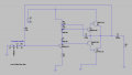
I am still trying to understand this circuit

upload_2018-1-14_7-0-57.png

where now I understand that the NFB is applied in parallel at the base and is reducing the input impedance of the input stage while the output impedance of the output stage is reduced.

With regards to the blurb about NFB applied to the collector. My point was just simply it is not possible. Adding or subtracting current or voltage to the collector does not affect the magnitude of the base current entering the transistor. The current that enters the collector of the transistor never changes.

On the other end of the feedback network, is the feedback current derived or voltage derived?

Thanks,
Chris
 
Top