 Facebook
 Google
 GitHub
 Linkedin
Hello im still building some basics circuits in order to learn yet.
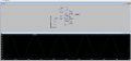
I have built a common emitter amplifier now, what i have assigned to myself is making a circuit that has as input a 6 AC Sine wave, and as output i want a 12V AC.
I chose a load resistance of 424 Ohm , so RC=424Ohm and supply voltage VCC is VCC=12V.
The calculations i did are these, i dont know exactly if its the best way to build such circuit or what exactly so feel free to tell me please.
IC(max) = (VCC-VRE)/RL = (12-1)/12 = 9.2mA ( here i chose the VRE to be around 10% of VCC so around 1V ), secondly the ic calculated is fine for the transistor i chose, which is the 2N2222 that can withstand 800mA as IC
After this i calculated the Q point with zero input signal applied to the base, which is Ic(max) / 2 = 4.58mA
Once i calculated this value, now i can calculate IB, i looked the datasheet and it says that the current gain is around 75 for an IC of 10mA, so as approximation we choose a beta of 37.5
ib=IC/B = 4.58mA / 37.5 = 122uA
Now instead of using a separate " resistor " to set the current at the base of the transistor, R1 and R2 can now be chosen to give a suitable quiescent base current
A general rule of thumb is a value of atleast 10times IB flowing through the resistor R2.
R2= (VRE + VBE) / 10*IB = (1+0.7)/10*122uA = 5.7kOhm
R1= VCC- (VRE+VBE) / 11*IB = 12-1.7/1342uA = 7.6kOhm
Now since i calculated IC and IB i can find IE, IE is equal to IE=IC+IB = 4.58mA + 122uA = 4.7mA
with this given i calculated then RE = VRE / IE = 1V / 4.7mA = 212Ohm
my output isnt as expected, i have no idea why this happens, anyone got any clue? Thanks!
Attachments
-
1.2 KB Views: 4
-
 45.1 KB Views: 20


