Common emitter npn Ib and Ic

Audioguru

Joined Dec 20, 2007
11,248
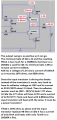
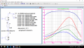
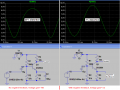
I am showing you that a 2N3904 does not have enough beta to properly drive a TIP32 so I am using a 2n4401. A 2N4403 replaces the 2N3906.

I am also showing you why driving the diodes is a nightmare and I fix it.
 

Attachments

Thread Starter

cmisip

Joined Sep 23, 2017
89
Thanks,
I am trying to understand this in stages.

The lack of linearity of the 2N3904 was something that I did not see in LTspice. The waveform looked fine. I don't know that LTspice can model this. Perhaps somebody could chime on that. I think LTspice uses a fixed Bf value for hfe. I checked a datasheet for the 2N3904 and the hfe does fall down at the higher Ic ranges. This leads me to the conclusion that it is best to pick a portion of the hfe vs Ic graph where the hfe is flat to use as operating range for a transistor. This is because we want to be able to have an equal proportion rise in Ic for every step rise in Ib at whatever Ib value. This means a near constant hfe. If the hfe reduced at higher currents, then the output sine wave would have a flatter or rounder top and hence will not be a faithful reproduction of the source AC input.

I am still fuzzy on graph interpretation on the datasheet. I am not sure how to interpret the different size line intervals. However, the tip32 datasheet seems to shows hfe falling quite a bit past 1 A.

Q1. Is the lack of linearity not a problem at the tip32 stage?

I also think that I am seeing the push pull stage at this time in a different perspective. It really is two CC stages stacked on top of each other ( stacked with regards to where they operate in terms of Vcc) . But they alternately share a common emitter resistor which is actually the speaker. It's easier to appreciate it if you think that you can ignore the other half of the circuit since that transistor is in cutoff anyway.

I stated in an earlier post that the emitter resistor in the CC stage seems to have too much current through it that is wasted instead of going into the load parallel to it. In the case of the push pull stage, the current is put to good use because the speaker becomes the load.

The speaker impedance then provides negative feedback. Too much current through it would mean too much voltage drop across it which means a smaller Vbe which means a smaller Ib which means a smaller Ic which means a smaller voltage drop.

I noticed you used the minimum hfe.

Q2. Is this then a rule of thumb with regards to designing amplifiers? That is, to always design with the minimum hfe in the datasheet.

Working with lower hfe's will make it easier to design a direct coupled version instead of base bias via voltage divider. The base current of the push pull stage input would be higher. The input impedance of the push pull stage would be lower. It would be easier to design a CE stage that looks like the appropriate base resistor to the push pull input stage. I will see if I can work on that.

Thanks,
Chris
 
Last edited:

Audioguru

Joined Dec 20, 2007
11,248
Chris,
A transistor is not a generator of current, instead it is a follower of voltage. Since all transistors have a range of beta where some are high and others are low, even if they have the same part number, then if you use the "typical" beta shown on datasheet graphs and used by a simulator then half of your circuits will not work because the beta is too low. Therefore always design circuits using the minimum values of beta so that all circuits work.
Biasing? A transistor is biased with voltage, not current. If you bias a transistor with a voltage divider to work if its beta is minimum then it works the same or a little better if its beta is high because the lower base current will not affect the bias voltage.You do not want low beta and the resulting high current. You want high voltage gain then more feedback can be used then the distortion is lower.

Did you notice in my attachment that driving the diodes instead of driving the transistors results in 12 times the current needed in the first transistor? It is wrong to drive the diodes but teachers always did it.
The 200mA 2N3904 works poorly above about 50mA so I replaced it with the 600mA 2N4401 that works well at 150mA.
 

Audioguru

Joined Dec 20, 2007
11,248
Most people can hear 0.5% distortion. I can hear 0.1% distortion or less.You might see 2% to 5% distortion on a 'scope.
All transistors produce distortion and beta linearity has little to do with it. Simply, if the beta or your current is too low then the maximum output level will be reduced causing clipping. Lots of voltage gain and lots of overall negative feedback reduce distortion to the vanishing point but that ain't gonna happen in this simple circuit.
 

OBW0549

Joined Mar 2, 2015
3,565
I checked a datasheet for the 2N3904 and the hfe does fall down at the higher Ic ranges. This leads me to the conclusion that it is best to pick a portion of the hfe vs Ic graph where the hfe is flat to use as operating range for a transistor.
Not really. We design amplifiers so they will work properly regardless of a transistor's beta, provided it exceeds some minimum value.

Trying to pick a "sweet spot" along the curve of beta vs. collector current is a waste of time and effort because of large unit-to-unit variations; as @Audioguru indicated, it's far more productive to start with an amplifier design having extremely high open-loop gain, albeit with some (or even a lot) of distortion, then giving it negative feedback through passive, linear components (i.e., resistors and capacitors) to set the overall gain.

The distortion, along with any variations due to unit-to-unit differences in transistor characteristics, is then reduced by a factor equal to the loop gain, which is the open-loop gain of the amp without any feedback, times the attenuation factor of the feedback network.

Much better results, much less work and uncertainty.
 

crutschow

Joined Mar 14, 2008
38,572
The lack of linearity of the 2N3904 was something that I did not see in LTspice. The waveform looked fine. I don't know that LTspice can model this.
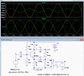
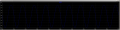
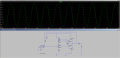
Here's an LTspice simulation showing the non-linear output of a common-emitter 2N3904 stage with no feedback (green trace, S1 closed), and the more linear output with negative emitter feedback (yellow trace, S1 open).
The distortion is caused by the non-linear relation between the large-signal base-emitter input voltage and the collector current of a BJT transistor (change in transconductance).
This is not directly related to the transistor Beta change with collector current.

upload_2017-12-31_22-19-59.png
 
Last edited:

Thread Starter

cmisip

Joined Sep 23, 2017
89
@Bordodynov
Thanks for chiming in on that point. The distortion then cannot be seen in LTspice where the distortion is caused by the hfe vs Ic curve not being flat as possible at the operation range of the transistor. So this type of distortion can only be seen when we connect an oscilloscope to an amplifier.
@OBW0549 and @Audioguru
So its better to design for lower hfe's. If I design for typical or higher hfe's and in fact the real transistor has a low hfe, then the gain would be lower than I expected. I can only do so much with positive feedback before I introduce too much distortion. If I design for lower hfe's and the actual transistor hfe is actually high, then I have more gain than I expected but then I have negative feedback at my disposal to reduce the gain. I would just be tweaking one resistor instead of a bunch of components to get to the gain that I was designing for.
@Audioguru
I did notice the analysis on the attachment. I will work on modifiying the schematic. What I don't understand is why you were concerned with the lack of linearity of the 2n3904 but not with the lack of linearity of the TIP32. Am I reading the datasheet wrong which implied the amplification is not linear at that level of Ic? Wouldn't it be better to use two tip32's at the shoulder to split the current load so that they both work in the flatter range of the hfe? I am either reading the datasheeet wrong or its implications or some other condition factored into your decision.
@crutschow
Thanks for that insight. I think I finally understand (maybe) how emiter resistor reduces distortion. Correct me if I am wrong, but at higher Ib levels, Ic does not proportionally increase as well as it did at lower Ib levels. Since the Ic is lower in proportion to the Ib at these higher Ib levels, the negative feedback is reduced, causing Vb to increase (hence Ib) just slightly to compensate for the reduced Ic. The effect is a less distorted sine wave.

Was my analysis of the push pull stage as being two parallel CC stages operating at different portions of Vcc <-> GND alternately using the speaker as emitter resistor accurate?

Thanks,
Chris
 

OBW0549

Joined Mar 2, 2015
3,565
If I design for lower hfe's and the actual transistor hfe is actually high, then I have more gain than I expected but then I have negative feedback at my disposal to reduce the gain. I would just be tweaking one resistor instead of a bunch of components to get to the gain that I was designing for.
No.

There's an important principle here which you seem unable-- or unwilling-- to grasp: negative feedback is not intended to provide you an easy means of "tweaking" the gain up or down to compensate for differences in transistor beta; it's there to make the circuit's voltage gain insensitive to transistor beta and eliminate any need for "tweaking" altogether. In a properly designed circuit, the voltage gain will be determined almost entirely by the feedback components, NOT semiconductor device characteristics.
 

crutschow

Joined Mar 14, 2008
38,572
I think I finally understand (maybe) how emiter resistor reduces distortion. Correct me if I am wrong, but at higher Ib levels, Ic does not proportionally increase as well as it did at lower Ib levels. Since the Ic is lower in proportion to the Ib at these higher Ib levels, the negative feedback is reduced, causing Vb to increase (hence Ib) just slightly to compensate for the reduced Ic. The effect is a less distorted sine wave.
Not there yet.
The reduction in distortion due to the emitter resistor has little to do with the base current or Beta, as I previously stated.
It is mainly a Vbe voltage-gain effect, not a Ib current-gain effect.
The emitter resistor reduces the non-linear relationship between the large-signal base-emitter voltage and the collector current as explained here.

Remember that the base-emitter junction appears as a forward biased diode, which has a logarithmic relation between voltage and current.
That is what causes the BJT output current to be non-linear with respect to the input base-emitter voltage.

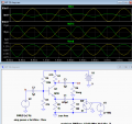
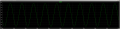
Below is the simulation showing the base input current along with the output voltage.
You can see that the input current is quite non-linear with voltage for the case with the bypassed emitter resistor, due to the non-linear input current vs. input Vbe.
That is what causes the distortion, not any variation in Beta.

upload_2018-1-1_8-58-3.png
 
Last edited:

MrChips

Joined Oct 2, 2009
34,946
The emitter resistor introduces negative feedback. In this case, negative feedback is beneficial because it reduces non-linearity and adds temperature stability (while reducing overall gain). (It also changes other things such as input and output impedance and frequency response.)
 

Audioguru

Joined Dec 20, 2007
11,248
A transistor without negative feedback produces horrible distortion when it has a large voltage swing. The levels are not high enough to cause clipping.
Here is a 2N3904 transistor operating at low currents where the hFE is not changing and without negative feedback its distortion at a high level is horrible. With the negative feedback created by the unbypassed emitter resistor (but the negative feedback could be done in other ways) the distortion is fairly low.
 

Attachments

Thread Starter

cmisip

Joined Sep 23, 2017
89
it's there to make the circuit's voltage gain insensitive to transistor beta and eliminate any need for "tweaking" altogether.
Sorry, there's two kinds of negative feedback being discussed. What I meant by "tweaking" is tweaking the negative feedback from the output push pull stage that is directed to the input of the CE stage which Audioguru showed in one of the earlier schematics. If there is clipping or square wave on the output, the solution was to reduce input voltage amplitude, or increase THIS type of negative feedback. The other negative feedback is the emitter degeneration type.

The emitter type of negative feedback is the one that adjusts against effect of temperature, hfe variations between transistors, and helps correct the nonlinear input current ( due to the input voltage not being linear with input current because BE is a diode).

I have not yet incorporated the changes that Audioguru suggested with regards to driving the transistors directly instead of the diodes.

Thanks,
Chris
 

Attachments

Audioguru

Joined Dec 20, 2007
11,248
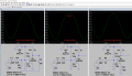
I show a transistor with collector to base negative feedback, no negative feedback with high distortion and emitter resistor negative feedback.

The two different types of negative feedback produce exactly the same voltage gain and exactly the same low distortion. DC negative feedback in addition to the AC collector to base negative feedback would be better so it can compensate the bias for temperature and replacement transistor changes.
 

Attachments

Thread Starter

cmisip

Joined Sep 23, 2017
89
Thanks,
There are three different types of feedback being discussed here now. The collector to base, the emitter resistor feedback, and the feedback from output of the CC stage to the input of the CC stage. I am not sure really what this third type of feedback is called.

@crutschow
Let me try it again. With the hfe constant, the input voltage is not reproduced exactly in the output voltage without negative feedback ( emitter resistor type ) because the relationship between Vbe and Ib is not linear. The relationship between Ib and Ic is linear ( when the hfe is constant). On the collector side, the resistor converts Ic to voltage which is the output voltage. So therefore, without the emitter resistor providing negative feedback, the output voltage will not be an exact reproduction of the input voltage.

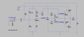
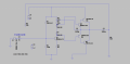
I have come up with this latest schematic which keeps the TIP transistors within the power dissipation allowed and it is a direct connection between CE and CC stage. The TIP transistors have 22 hfe, the 2N440's have 89 hfe and the 2N3904 has 70 hfe which are all the minimum hfe's I think.

upload_2018-1-7_22-0-59.png

upload_2018-1-7_22-1-47.png

The feedback from the output of the CC stage to the input of the CC stage drives the input voltage down to 100mv from 1 volt. The gain I think is around 100 on LTspice resulting in 100 mv to 10 volts. I was shooting for a gain of 1000 ( 10 mv to 10 volts ).

Can somebody check the calculations?
10 mv to 10 volts require a gain of 1000 so I needed a CE stage with an RC of 10*RE or 10*60 = 6000.
The gain of the CC stage is 21.12/21.82 = 0.9679 ( there is a .7 volt drop between the input and the output ). So I needed a resistor that looks like 6000 ohms for RC. 6000 = R / 1-.9679 ; R = 6000*.0321 = 192.6.

Why is the gain only 100 instead of 1000.
Why is the final output's peak voltage only at 8.26 volts while the negative peak is at 9.85?
Does bootstrapping the CE stage this way cause its output impedance to increase? (is it effectively 6000 + R3 now?) If so that might be the reason why the gain is lower than calculated as voltage will divide between the CE stage Zout and the CC stage Zin.

I just noticed that If I raise the emitter resistor of the CC stage to 800 ohms, and reduce the input to the CC stage to 10m, I could get 10 volts at the output of the CC stage so thats a gain of 1000. So the problem seems to be the input impedance of the CC stage. Any way to increase it without increasing the emitter resistor when the CC is directly connected to the CE stage? Also the output positive and negative peak seems equally centered at zero volts.

upload_2018-1-7_22-28-52.png
upload_2018-1-7_22-29-13.png

Thanks,
Chris
 

Attachments

Last edited:

Audioguru

Joined Dec 20, 2007
11,248
I am glad to see that the first transistor drives the output transistors, not the diodes.

You do not have overall DC negative feedback because R6 was connected to the grounded speaker instead of connected to the DC output of the amplifier. Then R1 and R2 are not needed and the value of R6 must be the correct resistance for symmetrical clipping at the output. The gain of the overall amplifier is roughly R6/R5.

You do not need such a high value for the bootstrap capacitor C2. Yes, bootstrapping causes the current in R7 to be almost constant resulting in a very high impedance collector load for Q1 and therefore high voltage gain for it. The value of R4 can be reduced for even more open loop voltage gain, a little higher output voltage swing and reduced distortion.
ou do not have DC negative feedback because R6 was connected to the grounded speaker instead of connected to the DC output of the amplifier. Then R1 and R2 are not needed and the value of R6 must be the correct resistance for symmetrical clipping at the output. The gain is roughly R6/R5.

You do not need such a high value for the bootstrap capacitor C2. Yes, bootstrapping causes the current in R7 to be almost constant resulting in a very high impedance collector load for Q1.
 

Thread Starter

cmisip

Joined Sep 23, 2017
89
You do not have overall DC negative feedback because R6 was connected to the grounded speaker instead of connected to the DC output of the amplifier
I thought I was only supposed to send back a fraction of the AC output in order to provide negative feedback and reduce the amplitude of the input to the CE stage. If I sent back the DC bias as well, won't that interfere with the DC bias setup at the base of the CE? I suppose if I remove R1 and R2, the DC bias of the CE stage would have to come from the DC negative feedback. This becomes like a chicken and an egg ( which comes first ) scenario but I could try that.

You do not need such a high value for the bootstrap capacitor C2.
I thought to send the full voltage back. I think If I used a smaller value capacitor, the capacitor would have reactance and reduce the voltage I send back to R7.

The gain is roughly R6/R5.
Is R5 supposed to be representative of the output impedance of the source. If this was line out of a PC then it might be around 24 ohms?

Thanks,
Chris
 

Audioguru

Joined Dec 20, 2007
11,248
I thought I was only supposed to send back a fraction of the AC output in order to provide negative feedback and reduce the amplitude of the input to the CE stage. If I sent back the DC bias as well, won't that interfere with the DC bias setup at the base of the CE? I suppose if I remove R1 and R2, the DC bias of the CE stage would have to come from the DC negative feedback. This becomes like a chicken and an egg ( which comes first ) scenario but I could try that.
When the 25VDC power supply is turned on some current goes through R3 to turn on Q5 which provides current to R6 that turns on Q1. The DC negative feedback stabilizes the output at the correct DC voltage.

I thought to send the full voltage back. I think If I used a smaller value capacitor, the capacitor would have reactance and reduce the voltage I send back to R7.
Make R3 and R7 both 330 ohms then a bootstrap capacitor of 220uF is good down to 30Hz.

Is R5 supposed to be representative of the output impedance of the source. If this was line out of a PC then it might be around 24 ohms?
Why overload the source? You NEVER match a load and a source for audio. The line output might have an impedance of 24 ohms but its minimum allowed load is probably 2k ohms. The output impedance of a modern audio power amplifier is 0.02 ohms or less but its minimum allowed load is 4 ohms.
 

Thread Starter

cmisip

Joined Sep 23, 2017
89
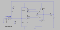
My gosh, the chicken and the egg they arrive at the same time!

upload_2018-1-8_23-3-50.png

I have to study this a bit. Could you provide a general explanation.

Thanks,
Chris
 
Top