Common emitter npn Ib and Ic

MrChips

Joined Oct 2, 2009
34,946
I think you are over-thinking this problem.
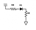
diode voltage drop.png

Look at the drawing above. It doesn't matter what are the values of Vbb, RB and RE.
As long as the diode current exceeds a certain threshold value, the voltage across the diode will be 0.7V, give or take 0.1V, especially for the base-emitter junction of a small signal silicon transistor operating in the linear region.

The point of negative feedback from the emitter resistor is that it is a self regulating mechanism, like a governor speed control mechanism.

In this case the current in RE will be hFE times the current in RB (with regards to a BJT). Hence when Vb tries to increase, VE increases to oppose Vb, hence the stabilizing effect.
 

OBW0549

Joined Mar 2, 2015
3,565
I am still trying to wrap my head around the concept of using a emitter resistor to ensure that variance in different transistor's Vbe (under different operating temperatures) could be negated with a single value of emitter resistor.
There are a few concepts in electronics, such as Ohm's Law, that are simpler than that, but not many. What you really ought to be doing is trying to wrap your head around the reason(s) why you are having such enormous difficulty understanding such simple things.

But I see on the simulator that increasing the emitter resistor seems to decrease the swings of Vbe so a lower value of emitter resistor results in a wider amplitude of Vbe, hence increased likelihood of meeting the Vbe of different transistors.
This statement, like so much of what you've written in both this thread and in the "pullup resistors" thread, makes absolutely ZERO sense. NONE. AT. ALL.

I just need to find the conceptual explanation for this.
Well, you're most certainly not going to find it by continuing to concoct fanciful, magical explanations on your own.

Find a good textbook or tutorial (the one right here on AAC is a good place to start) and discipline yourself to understand the material in the terms in which the material is presented to you rather than "conceptualizing" (as you call it) everything in your own idiosyncratic, error-ridden terms and faulty "logic", distorting it beyond all recognition.

It seems clear to me that you've certainly got the mental capacity to understand electronics and to do so quite competently, but you are preventing yourself from understanding through this nasty, self-defeating habit of rejecting (or at least ignoring) the explanations in whatever tutorial material you're using and substituting your own convoluted notions. If you expect to get anywhere, you simply MUST conquer that habit.

It all brings to mind the favorite t-shirt saying of Adam Savage on the old Mythbusters TV program: "I reject your reality, and substitute my own!" In electronics, you absolutely, positively CANNOT substitute your own reality for what you read in the textbooks. It simply doesn't work. The result is what I call "voodoo electronics."

So hit the books, pay attention, focus, and STOP trying to re-interpret everything you read. You've got what it takes, but you've got to apply yourself and get out of "thrash mode."
 

MrChips

Joined Oct 2, 2009
34,946
One of the goals of a good educator is to observe the problem from the perspective of the student and to encourage and divert the efforts of the student into a different perspective that yields a successful outcome.

The TS is fixated on analyzing the lowly BJT amplifier from a voltage perspective. The BJT is a current device. One analyzes the behavior of the BJT amplifier using current analysis.

In contrast, the FET is a voltage device. A voltage analysis works better with an FET amplifier.
 

Audioguru

Joined Dec 20, 2007
11,248
Cmisip,
The Hobbyist posted two circuits, the first one has the transistor saturated but the second one is biased correctly so that the collector voltage is 2.617V. Since every transistor has a different Vbe and differing temperatures then it won't work with many transistors like the one in your simulation unless you fiddle with the resistor values or add negative feedback.

Negative feedback reduces the voltage gain so that if a transistor is used that is saturated without negative feedback, then with negative feedback it will not amplify so much and it will NOT be saturated. If a transistor is cutoff without negative feedback, then with negative feedback it will not amplify so much and it will NOT be cutoff.

The base bias resistors do not hold the base voltage steady, instead they bias the input with the correct voltage and current then the input signal can swing the base voltage up and down. When the base voltage is increased by the signal then the base current increases which causes the collector current to increase much more causing the collector voltage to drop. When the base voltage is decreased by the signal then the base current drops which causes the collector current to drop much more causing the collector voltage to increase.
 

hobbyist

Joined Aug 10, 2008
892
The way I see it, there is no way to drop the voltage at the collector to 2.617 volts. If I trace a path from the 5 volt supply to ground on the collector side, I only see one resistor to drop the voltage so the voltage drop there must be close to 5 volts leaving only a few millivolts on the collector. We cant satisfy Vc > Vb.
Yeh I see where it looks confusing when your new to transistor circuits.

Your use to seeing a resistor dropping voltage as current flows through according to ohms law, but it is hard to picture the transistor dropping voltage across it the same way, the transistor in its linear state acts as a variable resistor, thats why its important to bias it on where the base current curve is in the linear region on the collector charactersistics, because transistors vary in manufacturing tolerances, it is always good practice to bias the transistor to be as independant of inherent parameters as possible, that's why negative feedback is used via collector feedback or emitter feedback, and base divider networks are used to stabilize base voltage ect...

A resistor can only be variable by changing its physical resistance, a transistor varies its apparent resistance by the current input to its base terminal, the transistor is not a physical variable resistor, but it (acts) as a variable resistor, by the current flow allowed by its input to output relationship.

So just as you manually change the resistance of a variable resistor by turning a knob, in the same respect, you are able to change the apparent resistance of the transistor by changing its base current input.
 
Last edited:

Thread Starter

cmisip

Joined Sep 23, 2017
89
Thanks guys,
Thank you for your patience and thank you even for just taking the time to answer the post.

I am not ignoring anybody's post. I am just trying to assimilate them all into one cohesive model. The memory part of my brain does not work as well as the story part. I am slow to spit out facts because the story in my brain has to play out and I derive the facts from there. Even the story part will take fantastical journeys until I understand a concept and therefore tone it down to something saner. It is a process that will continue to get saner and saner I hope as I find the right model. Any new information that conflicts with the model's prediction imply that something is wrong with the model or that something is wrong with the new information or that I am simply missing a part that connects the two. A real test of the model is if it can predict things outside of what it was originally conceived from.

My misconception about the base voltage being constant is from this snippet from Electronics tutorials. They are not wrong. I just didn't understand. And so the model went into a fantastical journey.

"Since the base is held constant by the divider resistors R1 and R2, the DC voltage on the base relative to the emitter Vbe is lowered thus reducing the base current and keeping the collector current from increasing. A similar action occurs if the supply voltage and collector current try to decrease."

Likewise Vb = Ve + Vbe which is correct, put in the notion of Ve being a floor that pushes up and down Vb.

The following is definitely wrong and must be rejected. I did observe it but the story is wrong. I think though I am getting closer.

"But I see on the simulator that increasing the emitter resistor seems to decrease the swings of Vbe so a lower value of emitter resistor results in a wider amplitude of Vbe, hence increased likelihood of meeting the Vbe of different transistors."

--------------------------------------------------------------------------

So far I think this is what is happening. hobbyist's explanation and MrChips latest diagram cleared things up a bit. And I think I even found AudioGuru's explanation to meld with this. Please correct me if I am wrong.

The base voltage determines base current. As the base voltage increases, so does base current Ib. The increase in Ib causes an increase in Ic (hfexIb) by lowering the resistance of the CE junction. From Vcc to GND on the collector side, the voltages must drop all the way to zero. The CE voltage drop is controlled by the setting of its "variable resistor" through Ib. The voltage drop on the collector resistor and the emitter resistor must proportionately share the remaining voltage. Because the emitter resistor is smaller than the collector resistor and the current through both can be assumed to be almost equal ( Ie is just slightly higher than Ic), the voltage drop on the emitter resistor would be smaller than the collector resistor. The emitter resistor is in the first loop as well with the BE and the base resistor. From Vcc to GND, the voltage must drop all the way to 0. So the base resistor, the BE junction, the emitter resistor must proportionately share all the voltage drops. If on the collector loop, the emitter resistor voltage drop increases ( happens when the CE voltage decreases (V=IR with R reducing) which is because the CE resistance decreases (R reducing, Ic a function of Ib and is constant for this snapshot in time) which is due to base current increases which is due to base voltage increases ), it must cause the base voltage to decrease. Hence the negative feedback. On the simulator, the Vbe voltage does fluctuate minimally. I assume that it is because it is also a resistor or it is a diode with a small resistor on its tip. If that is the case, then without an external emitter resistor, the shift of voltage drops between the base resistor and the small emitter (internal) resistor would cause significant or near Vcc drops through the base resistor, which might lower the base voltage below the threshold of .7v. Increasing the emitter resistance with an external (to the transistor) resistor would ensure that the voltage division between all three resistive components never results in too big a drop on the base resistor that would cause the base voltage to fall below .7 volts. So enough negative feedback ensures that the transistor remains in the FWD active mode.

Thanks,
Chris
 

hobbyist

Joined Aug 10, 2008
892
From Vcc to GND on the collector side, the voltages must drop all the way to zero.
The transistor will never drop to zero across its CE terminals, but will drop to a value due to its make up in the millivolt region.
That's where the term for voltage saturation region comes in, all in all your getting a good handle on this.
 

Thread Starter

cmisip

Joined Sep 23, 2017
89
Thanks, I meant the sum of all voltages from Vcc to GND on the collector loop must drop to zero. But there is a small resistance even when the transistor is fully on that accounts for a small voltage drop across the CE junction at saturation. Again It is easier to think of it as a small resistor in series with the emitter because it is common to both the collector side and the base side.

Thanks,
Chris
 

hobbyist

Joined Aug 10, 2008
892
Thanks, I meant the sum of all voltages from Vcc to GND on the collector loop must drop to zero.

Thanks,
Chris
Yes , from theses last couple posts, i would say you have a very good knowledge of transistor operation, now start doing experiments using real components, and test out things, you can really learn a lot about transistor behavior when you do the actual circuit designs and tests.

I admire your persistance in pursuing, to get a full understanding in transistor actions before moving on to advance design using neg. feedback and such.

Ive found in transistor circuit design, that getting a good understanding of why the theories (rules of thumb) work, takes one step at a time, then when you understand why they work, you have a better appreciation for how to work with those theories to design circuits, that will actually work, according to your calculations that gets you close to expected values.

Transistor circuit design, at a hobby level at least, is calculating expected values, building the circuit, then tweeking to get expected values if reasonable, where the calculations are always to get you in the ballpark, its the final tweeking that makes the circuit complete.
 

Thread Starter

cmisip

Joined Sep 23, 2017
89
Thanks again. I've found out that this model explains more than the facts It was originally conceived from.

1. Reducing Vcc would reduce Vb, reducing Vbe, reducing base current, reducing Ic, reducing Ie, reducing the voltage drop at the emitter resistor, making base voltage want to go up ( negative feedback stopping further degradation of base current, basically voltage stabilization at the base).

2. Siphoning off the current at the collector ( by adding a node ), thus reducing Ic, reduces Ie, reducing emitter resistor voltage, increasing Vb, increasing Ib, increasing Ic. Again, negative feedback regulates against a increased load between collector and GND. Basically current stabilization at the collector side.

3. The use of a bypass capacitor on the emitter resister, shorts it out for frequencies that are allowed to pass through the capacitor, negating the emitter voltage drop, removing the negative feedback on the base voltage (and current) so that the signals we want to amplify will have good gain ( as negative feedback reduces gain). Outside of the frequencies (unwanted frequencies) that the bypass capacitor is rated to pass, the emitter resistor will have current through it and therefore will exert negative feedback, reducing gain so we are not amplifying noise for example or any unwanted frequency.

4. With number 3 above, it is important not to negate the desired effect of raising Vb so we exceed the transistor's required forward voltage drop at the Vbe junction by a safe margin to account for variation in Vbe due to manufacturing process or temperature. So it makes sense to have two resistors in series. One to keep the Vb at the desired voltage level to keep the transistor working in FWD Active (by negative feedback ), and another in parallel with a capacitor to negate ( at least partially, since the other resistor is still in play ) the negative feedback for frequencies we wish to amplify.

I may have extended the model past what it can explain or predict. I hope the above is accurate but I could be wrong. I am just spouting a quick analysis.

Thanks,
Chris
 

OBW0549

Joined Mar 2, 2015
3,565
...
I may have extended the model past what it can explain or predict.
A little bit.

Regarding point #2, you've made it unnecessarily complicated and missed a VERY important point: in a BJT, for any given Vbe (or Ib), Ic remains nearly constant against changes in Vce (except for the Early Effect, which is usually negligible). So adding a resistive load to ground at the collector doesn't "siphon off" collector current; it merely drags down the collector voltage with little or no effect on the collector current.

Points #1. #3 and #4 are kinda-sorta OK. Over-thought, but OK.
 

Thread Starter

cmisip

Joined Sep 23, 2017
89
Thats kinda what I meant. Adding a resistive load at the collector to ground provides a parallel route to the current. However Ic will not change despite current flowing through the resistive load because of negative feedback. Vcc must again drop to GND after the "node" through the resistive load. The resistive load becomes a parallel resistance to CE and the emitter resistor effectively reducing the resistance after the "node". This will have the effect of reducing the voltage measured from the collector to GND. The resistive load must be high enough to still maintain Vc > Vb. If its too low, the voltage division will favor the collector resistor, lowering Vc. The increased current draw will be evident on the supply at Vcc before the current divides between the base side and the collector side but it wont be seen at Ic. So while you provide current to the resistive load, Ic remains the same.

Unless, I made another mistake here.

Thanks,
Chris
 

OBW0549

Joined Mar 2, 2015
3,565
However Ic will not change despite current flowing through the resistive load because of negative feedback.
Nope. Wrong.

Ic does not change because collector current is almost entirely independent of changes to Vce. Negative feedback has absolutely nothing whatsoever to do with it in this case; this is a characteristic of the transistor itself.
 

Audioguru

Joined Dec 20, 2007
11,248
I think Chris meant that adding a load at the collector causes the effective collector load resistance to decrease which decreases the voltage gain and negative feedback cannot fix that.
 

OBW0549

Joined Mar 2, 2015
3,565
I didn't get that from what he said. He said, "2. Siphoning off the current at the collector ( by adding a node ), thus reducing Ic..."

If he meant something else, I figure he would have said so.
 

hobbyist

Joined Aug 10, 2008
892
Chris, please explain what you mean by negative feedback, because in transistor circuit design of DC bias (getting the transistor in the active region) is done either as series current feedback, or voltage shunt feedback.

(example NPN transistors)
Series feedback is where the Emitter resistor is used, as the transistor heats up and wants to go into thermal runaway the extra current draw through the emitter resistor cause the voltage drop at the top of the resistor to become more positive,(NPN) thus reducing Vbe so the transistor base current then becomes less wich in turn allows less collector current which in turn allows the Vbe to stabilize. Since the current is the factor in this it is in series with the base emitter junction then its called "series current negative feedback".
As you study further into this by experimenting, you will discover that you can design the gain of that stage by choosing appropriate emitter and collector resistors.

Shunt voltage feedback is when you choose to use only one resistor for base bias, but instead of connecting it to the Vcc, you connect the resistor from base to collector, then you use your chosen collector voltage to determine the value of this resistor.
The feedback happens as a voltage rather than a current, again as transistor begins to conduct excessive collector current due to thermal runaway, the collector voltage drops considerably(NPN) this puts a drop on the base voltage since now the collector voltage governs the base voltage, so this decrease in base voltage causes the transitor to conduct less until equilibrium takes place and becomes stable again.

Both of these are what is commonly known as negative feedback, in DC bias design.
I say DC because there is AC feedback as well but that's other involvements.

Once you understand how emitter negative feedback works, you can then advance to emitter bypass capacitors for AC gain, but first learn how to design DC bias transistor circuits, before you start designinjg AC circuits.

When you can take any transistor BJT, and calculate values for all resistors then build and tweek the values and know why the tweeking was necessary, then you are ready to design small signal transistor amplifiers.
 

Thread Starter

cmisip

Joined Sep 23, 2017
89
I meant adding a load connected from the GND to the collector. I thought negative feedback would cause Ic to be stable against that load. However, Ic is solely a function of Ib. Point 2 is wrong.

The only other use of negative feedback that I could see would be to guard against thermal runaway as you guys pointed out. When hfe increases due to increase in temperature of the transistor, the Ic current increases more than normal for each Ib increase, the CE voltage contracts more than normal, the collector and emitter resistor drop increase more than normal. With the emitter resistor, its top is more positive. With the collector resistor, its bottom is more negative. The effect of the emitter resistor would then be to reduce Vbe, reducing Ic. This is the negative feedback mechanism that I was talking about.

Let me see if I understand the shunt voltage mechanism that hobbyist was talking about. If a resistor was connected between the collector and the base and Ic increased due to temperature rise, then a more than normal drop on the collector resistor would cause its lower end (collector) to have a more negative voltage, and since this is connected to the base, a more negative voltage is added to the base voltage, this would reduce the base voltage, thereby reducing Ib. Hope that's correct.

The other thing that I thought I'd mention was the bias voltage at the base needing to be high enough to allow the negative swings of the input voltage to still keep Vb above .7 volts. Otherwise, the transistor would be in cutoff mode during the negative swing. So it seems the base voltage should be higher than just the sum of the emitter resistor voltage and Vbe. I am looking at the simulator and I see the input capacitor doing the job of raising the input voltage such that the peak of the negative phase is above zero as if a DC voltage was added to the AC signal. Without the input capacitor, the input voltage swings positive and negative. I am not understanding how this is working.

Thanks,
Chris
 

OBW0549

Joined Mar 2, 2015
3,565
The only other use of negative feedback that I could see would be to guard against thermal runaway as you guys pointed out.
Actually, thermal runaway is rarely a consideration other than in situations where a lot of power is involved-- mainly in high-wattage audio power amplifiers and such. Far more often, the main function of the emitter resistor is simply in stabilizing the DC operating point of the transistor and making it independent of variations in individual transistor characteristics such as current gain and base-emitter voltage drop.

Let me see if I understand the shunt voltage mechanism that hobbyist was talking about. If a resistor was connected between the collector and the base and Ic increased due to temperature rise, then a more than normal drop on the collector resistor would cause its lower end (collector) to have a more negative voltage, and since this is connected to the base, a more negative voltage is added to the base voltage, this would reduce the base voltage, thereby reducing Ib. Hope that's correct.
That's correct, though unnecessarily complex: increased collector current results in lowering the collector voltage, which means less voltage across the collector-to-base biasing resistor, which results in less current through the resistor and into the base, which results in reduced collector current. Voila-- bias stabilization.

The other thing that I thought I'd mention was the bias voltage at the base needing to be high enough to allow the negative swings of the input voltage to still keep Vb above .7 volts. Otherwise, the transistor would be in cutoff mode during the negative swing.
All this means is that whatever is driving the base of the transistor (e.g., the previous amplifier stage) has to refrain from overdriving it and thereby causing cutoff and/or saturation.

So it seems the base voltage should be higher than just the sum of the emitter resistor voltage and Vbe.
You lost me here. ???

I am looking at the simulator and I see the input capacitor doing the job of raising the input voltage such that the peak of the negative phase is above zero as if a DC voltage was added to the AC signal. Without the input capacitor, the input voltage swings positive and negative. I am not understanding how this is working.
The capacitor simply allows the base of the transistor and whatever is driving the amplifier to be at different DC potentials, nothing more. Without the capacitor, we would be designing a "direct-coupled" system; and designing direct-coupled, multistage amplifiers with very high gain is kinda tricky. Far easier to use a coupling capacitor between stages, so they are independent DC-wise.
 

Thread Starter

cmisip

Joined Sep 23, 2017
89
"
So it seems the base voltage should be higher than just the sum of the emitter resistor voltage and Vbe.
You lost me here. ???"

Sorry, dont know how the quoting system works. What I mean is doesn't the AC input just get added to the voltage at the base. The AC input swings voltage positively and negatively. Its like adding a series battery source and then flipping the battery over on the negative swing. Whatever voltage is at the base increases in the positive swing and decreases in the negative swing. If the voltage in front of the Vbe junction falls below .7 v because we are in the negative swing, the BE junction wont be forward biased.

Thanks,
Chris
 

OBW0549

Joined Mar 2, 2015
3,565
What I mean is doesn't the AC input just get added to the voltage at the base. The AC input swings voltage positively and negatively. Its like adding a series battery source and then flipping the battery over on the negative swing. Whatever voltage is at the base increases in the positive swing and decreases in the negative swing. If the voltage in front of the Vbe junction falls below .7 v because we are in the negative swing, the BE junction wont be forward biased.
Correct! You've got it.
 
Top