Common emitter npn Ib and Ic

hobbyist

Joined Aug 10, 2008
892
The analysis looks good I guess, (still on post #98), however can we please get back to the starting point of designing a CC amp. as posted in post #93.

Your getting way ahead of yourself when your talking about CC darlington pair.

First of all, the circuit design I did in post #75 pointing to "lesson 3" was just an excersise in biasing transistors for determined currents and voltage references, and at the end be able to turn it into a audio amplifier to drive a 8 ohm spkr.

To design a transistor power amplifier, it is common to use a class AB configuration to achieve power efficiency as well as hi fidelity output.

I have just made another very effective audio amplifier using all 2n3904's with DC coupling, where each transistor stage takes the place of a bias resistor for the stage it drives, exercising learning how to bias transistors and still have a usefull amplifier at the end.

So my designs are not failures per say, but they are not the norm, in power amplifiers used to drive heavy spkr. loads, as you are suggesting about spkrs. in parrallel and such.

That's why I keep saying go back to the very basics of amp design, starting with post #93, I posted pics. of the texts I learned this from so you can read the design steps, then I used those design steps to design a simple CC amp. that worked according to design requirements.
Do not use a spkr. but start out by developing a signal voltage (nondistorted) AC coupled, across a pure resistance, if you use a resistor you can see how the transistor handles a resistive load, then change it for a spkr. load, to see how the circuit responds.

Build or simulate that design with the component values I used, then begin changing values of ,load, VCC, base resisor, emitter resistor, and see how the circuits performance changes.

Once you get a good grounding of understanding the in's and out's of that simple stage, then you can have a better idea how to couple that stage, with Zout of other stages be it AC coupling, or DC coupling.

From there we can take it slowley, adding to it a couple of preamp stages all DC coupling to get a feel for BIASING transistors, and learning how and when to use bypass capacitors, when and how to use miller caps. to eliminate unwanted oscillations, then finally when you have an actual working amplifier, with stability in component changes and temperature, ect..
then you should be ready to design AC coupled stages, then finally in the audio range, and actual class AB power amp, that you could use to drive spkrs. to high DB of voume with no distortion.

But it all starts with the basics. If you have any questions concerning the design steps in post #93 I'll help you with it.
But all these other questions your asking in the newer posts, someone else can help you with, as it is beyond my expertise, as this is only a hobby for me.

ps: I'll look over your last post, and try to answer anything I can, however please consider what I wrote above.

Thanks.
 

hobbyist

Joined Aug 10, 2008
892
Is there just not enough current?

Take 10v pk across 8 ohms, = 1.25 amps.
How much current is Q4 supplying, for the positive excursion, and how much is Q4 shutting off to allow Re to sink current needed to drive 1.25 amps into the 8 ohm load for the negative excursion.
 
Last edited:

Audioguru

Joined Dec 20, 2007
11,248
R8, R9 and R10 are wrongly measured in uF.
The small 2N3904 transistor for Q4 has a maximum allowed collector current of 200mA and a max heat dissipation of 0.625W. Its heating is (25V - 11.1V) x 110mA= 1.53W and the peak current will try to be 1.46A. Its current gain drops pretty bad above about 50mA and it will smoke and burn in this circuit of a class-A heater.

If you want a class-A heater then you need a power transistor for Q4 so that it can pass 1.46A peak and heat with 1.53W. A TIP31 would be fine without a heatsink and will have a minimum current gain of about 15 then Q3 would have a peak collector current of 100mA and it will need to be more powerful than a 2N3904, maybe a 2N4401. Then the peak collector current of Q2 will be about 1mA. When the collector voltage of Q1 tries to swing 10V peak up to 23V the current from R1 is only 2V/10k= 200uA but the base current of Q2 needs to be only about 14uA which will not reduce the output voltage swing much.

The 1uF of C2 has a reactance of 160 ohms at 1kHz so it reduces the output across the 8 ohm load to 1/21th. The first schematic has 100uF for C2 then it reduces the output level to about 0.83 times.
There is no negative feedback so this amplifier will sound awful.
 

Thread Starter

cmisip

Joined Sep 23, 2017
89
@hobbyist

This is what I did.
The voltage span I want at the output is 10 volts peak or 20 volts peak to peak .

20 volts / 8 ohms = 2.5 A x 1.2 = 3A IL

25/2*3 = 4.17 ohms RE

I tried this first but was not getting the output I expected. So I tweaked the RE to no avail. 4 ohms or 100 ohms RE have the same result. However, I did not consider the reactance at all. I have to read up on that. I just assumed any capacitor would work.
I also thought the input impedance to the CC stage was high enough to not have to worry about the CE stage Vout dropping. So I just used the Q point of the CE to base bias the CC stage.

@Audioguru
The resistors you mentioned are .0001u ohms. LTspice requires resistors to show currents so I put the value very low to not change the circuit. Like I said, I completely ignored the effect of capacitance. Now that I am playing with it just changing values and frequency, I can see that the voltage output is increasing. I will have to read up on this.

Thanks,
Chris
 
Last edited:

Audioguru

Joined Dec 20, 2007
11,248
The reactance of a capacitor is its AC resistance at a certain frequency and its reactance increases at lower frequencies.
If your load is 8 ohms then maybe you want the reactance to be 8 ohms at 100Hz. At 100Hz the signal across the 8 ohms load will be -3dB or 0.707 times the signal at the input of the capacitor. It is calculated as 1 divided by (2 x pi x frequency x resistance) which is 200uF. It will pass 1kHz with a fairly small attenuation.
 

hobbyist

Joined Aug 10, 2008
892
20 volts / 8 ohms = 2.5 A x 1.2 = 3A IL

25/2*3 = 4.17 ohms RE

I tried this first but was not getting the output I expected. So I tweaked the RE to no avail.
Ok I see your using the equation (1.2 x IL) for IE, so you are starting from the basics, now lets take this into a real design.

As a designer you need to read the data sheets for the transistor your using, google data sheet for a 2n3904, and check the HFE factor for IC for the transistor, the reason you will not realize a voltage gain across the 8 ohm load as your expecting, is because you have to be able to supply the current through the transistor. (2n3904 is a small signal gen. purp. amp)
The HFE changes dramatically at high currents, so you will run into problems getting base current needed.

As a designer you will need to research out a transistor that can handle the amont of current you want to use, then check its HFE values and work around that,
Hint,: always use the minimum value shown to do your design with.

Once you get the right transistor for the job, then you can begin working on frequency selective capacitance and such, these are just some hints to keep you from getting discouraged when your designing circuits.
 
Last edited:

hobbyist

Joined Aug 10, 2008
892
Maybe this will better explain the difference in using the right transistor for the job.

Using beta min. 100 for calculations, showed base resistor needs to be =~360 ohms.
However due to IC out of 2n3904 range the beta ends up being =~(0.922 / 0.055) = 16.7 for HFE.

No load yet applied yet waveform is clipped on the neg. side. this is because of the voltage at the emitter =3.8V and input voltage is 8V pk. So transistor is conducting enough to allow the positive pks. but due to low emitter voltage with respect to input, it cannot finish through the neg. side of the signal.

2n3904 b=100.jpg


How to fix this, lower base resistor to allow more current to flow in emitter to bring voltage at the emitter up enough to handle input voltage.
Base resistance reduced now to 36 ohms. Also the load is applied and there is somewhat more symetrical output on the scope.
Note emitter volatage is around 10.6V so more neg. excursion can get through with the large 8V pk excursion input.

But what is the beta around now, (2.452 / 0.270) = 9 so HFE is reduced even further due to the transistor makeup of being a small signal amplifier.

2n3904 b=9.jpg


Now I replace the small signal 2n3904 for a higher power transistor, ztx869, then I look up on its data sheet the min Beta for a range of collector currents, then calculate and tweek the base resistor value to give me a good emitter voltage of 11.7V

My collector current is 2.98A, and I have a HFE =~ (2.98A / 6.59mA) = 452, which is around the value of the transistor HFE for that amount of collector current.


ztx power transistor.jpg

Circuit design tip:

Choose a transistor to match the currents and power needed for it to be used in.

This transistor can handle a large load like this with large input signal.
 

Thread Starter

cmisip

Joined Sep 23, 2017
89
I was also thinking that the problem with too much current at the output could be used by using multiple parallel transistors ( with higher amperage rating ) that are being fed by the emitter of the first CC stage. Then connect all their collectors together in sziklai configuration to sum up their individual collector currents to a large value that can accommodate the load requirements. Putting these parallel transistors in sziklai willI save .7 x 2 Vbe drops. Also, I think the capacitor before the load, does not become technically a short with AC but will present as a resistor dependent on the frequency of the sine wave. As such voltage divides between the capacitor and the load when there is AC. I am thinking I will replace the capacitor with a calculated ohmic resistance value equivalent to what the capacitive reactance would be and use that in series with the load resistor for determining IL. Therefore, the 8 ohm load might look like 10 ohms to the CC stage.

I will have to try this on the falstad as well because LTspice doesn't let me change the value of Beta. For the 2n3904, it defaults to 305. And it doesn't have the TIP transistors.

Thanks,
Chris
 
Last edited:

Audioguru

Joined Dec 20, 2007
11,248
I have never seen a little transistor like the ZTX869 that has such a high maximum allowed current and such a high beta at the high currents. Its maximum peak current is 20A(!) and at 5A its minimum beta is 250.
BUT, in the simulation its current is 2.98A and it has a voltage across it that is 24V - 11.97V= 12.03V so it heats with 2.98A x 12.03V= 35.85W. I would like to see a video of the spectacular explosion and fire caused because its maximum allowed heating is only 1.2W to 1.58W depending on how much copper is on its pins.
I mentioned the heating because this circuit is a class-A heater, not an audio amplifier. The maximum output power into an 8 ohm speaker is only 4.07W when it is barely clipping.

Cmisip, what is the function of the output capacitor? It passes audio to the speaker. At most audio frequencies its reactance is zero so it produces no loss. BUT its main function is to block DC so that the speaker cone is not pushed over to one side causing severe distortion and maybe burning out the speaker.
For an 8 ohm speaker a 2000uF capacitor will barely reduce the level of frequencies below 20Hz and most speakers cannot produce frequencies that low anyway. Amplifiers with a dual polarity supply have their DC output averaging 0V so the output capacitor is not needed.
 

hobbyist

Joined Aug 10, 2008
892
I think the capacitor before the load, does not become technically a short with AC but will present as a resistor dependent on the frequency of the sine wave.
Yes that is called capacitive reactance, however a resistor has the current in phase with the voltage across it, while reactances are out of phase, so you may run into some difficulty trying to analyse voltages and currents due to that phenomenon, because a capacitor coupling is to keep DC biasing seperate from stage to stage.
Resistor coupling is DC coupling of the load, which will upset original biasing.

However I congradulate you on your attempts to take this apart piece by piece to get your understanding of it, to satisfy any curiosity doubts you run into, that's how I learned at the very start, I bought those radio shack kits, build the circuit the right way, then began experimenting taking out components, until the circuit stopped working, then changed values according to my curiosities of how it would perform, until I finally got it designed my own way where I understood the basics of making it work.

Then took lots of notes, for every component change, ect... until I could build the circuit my way and get it to work on my understanding, rather than just copy a build out of someone elses idea.

Experimenting as your doing is the best teacher.
Keep up the good work.
 
Last edited:

hobbyist

Joined Aug 10, 2008
892
Chris, this thread has really stretched my enthusiasm to design a audio amplifier to drive a 8 ohm spkr. to audio output level, using (thanks to your thread) DC coupling between the stages to bring the load impedance up, enough so all I need is one preamp AC coupled stage for input small signal gain.

Because of that, I took the simple CC amp I was using in the lesson in post #93, used the methods I learned from this thread on DC biasing and added to this amp, and built a small signal audio amp. that is audible across the room to listen to the sound of electronic circuit switchings inside my cell phone, by just laying the cell phone on top of the input spkr.

I want to share this video with you, hoping it will spark excitement in you to try to design these kind of transistor circuits, using the basic knowledge you have of ohms law and transistor characteristics.

Here is a link to the video demo. in this blog.
This is a CC. transistor amplifier output to drive a 8 ohm transistor radio type spkr, using spkr.s as input and output

https://forum.allaboutcircuits.com/xfa-blogs/hobbyist.27220/


I design my circuits at the hobby level, so anybody who has basic knowledge of electronics can get these kind of results too.
That's the whole purpose of wanting to help those who are starting out, if I can get these kind of results at the hobby level, than so can you, I want to show that transistor circuit design at the (HOBBY LEVEL), is not formidable, and can be fun to play around with.
 

Thread Starter

cmisip

Joined Sep 23, 2017
89
@hobbyist
Thank you for sharing that. Its nice to see designs come to practical fruitions. I remember buying electronics magazines when I was a kid and assembling the kits. It was a lot of fun to see them work. When they did not work, I was at a loss. I got busy with other pursuits and study and work. Now I am interested in going back to this hobby but this time I want to be able to reason out why things don't work or how things work. I want to learn the theory as much as possible at the hobbyist level. This along side my interest in computer programming and mathematics. I seem to go in spurts. Right now its electronics. In a few months it may be C++ again. They are all puzzles that I can pick apart. One of these days, I will try to build these circuits. For a while I was messing with the Irobot platform and sensors and such. The interfacing of these sensors to the raspberry pi got me started in this direction initially with trying to understand pull up and pull down resistors. There are howtos out there but I want to be able to understand why things were done a certain way. Its a lot of fun.

I kinda ran out of time this weekend to complete the design I proposed. I ended up just tweaking what I have and adding the sziklai to reduce individual transistor currents. I understand that the 2SAR542P are past their power ratings. I used only 4 and I need 6.5 A for the load. What transistor can accomplish this?

I managed to get 8+ volts peak ( 16 volts peak to peak ) on the 8 ohm resistor. I am not sure what speaker power specification can handle this. I am just guessing. I think it might be 8/1.414 = 5.65 VRMS with a power delivery of (5.65*5.65)/8 = 4 Watts. The 8 ohm resistor current swings from 1 A to -1A. A greater portion of the current swinging from 1.12 to 5.5 A is across the 4 ohm emitter resistor. This part is still not clear to me but I think it is current division with parallel resistances. A lot of power is wasted on the emitter resistor. It seems it would be better to just put the 8 ohm resistor directly on the emitter in place of the emitter resistor. However, LTSpice seems to take a long time to simulate this unless I remove the capacitor. But without the capacitor, how do you remove the bias? I think I got the correct emitter resistor value at 4 ohms as per the howto posted. I can verify that this procedure for determining the emitter resistor works with different speaker impedances ( 16 ohm speaker required 8 ohm emitter resistor ) with only minor tweaking. The ratio is preserved for other impedances ( 32 emitter resistor required for 64 ohm load ).

The CE voltage swing for the 2SAR542P is 20.5 to 2 volts with a current swing of 0 to 1.64 A. I calculated maximum power as the product of the mid point voltage and current or ((( 20.5 - 2 )/2)+2)*(1.64/2) = 9.22 W, way above their rating. If I can successfully add the TIP125 spice model then I think that might be ok. I am not sure how to read the TIP125 datasheet though as there are two power ratings. There is
@ TC= 25°C = 60 W
@ TA = 25°C = 2.0 W
If the first line is what meets the conditions, then 9.22 W is way below that. I could be wrong. If its the second line, it will get toasty.

I replaced the 2N3904 with 2N4401. Its CE voltage swings from 20-2.26 and its current swings from 0 to 25.66mA. I calculated its power rating to be ((( 20 - 2.26 )/2)+2)*((25.66/1000)/2) = 0.1394621 W which is below the 625 mW rating. When I did the switch, the plots of current and voltages got better, indicating to me that LTSpice is considering component quirks when it runs the simulation. Both devices were operated below their maximum rating but the 2N3904 was close to its maximum and perhaps was not as linear in that range.

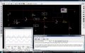
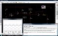
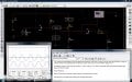
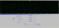
upload_2017-12-17_19-3-13.png

Thanks,
Chris
 
Last edited:

OBW0549

Joined Mar 2, 2015
3,565
I am not sure how to read the TIP125 datasheet though as there are two power ratings. There is
@ TC= 25°C = 60 W
@ TA = 25°C = 2.0 W
If the first line is what meets the conditions, then 9.22 W is way below that. I could be wrong. If its the second line, it will get toasty.
Those two ratings on the TIP125 data sheet,

Untitled.png

are very common; you see them on most semiconductor devices. The first one, the rating at Tc = 25°C, gives the maximum allowable dissipation with the case temperature held at 25°C-- that is, with the metal tab of the transistor mounted firmly to an infinite heat sink.

The second one, the rating at Ta = 25°C, gives the maximum allowable dissipation with the device standing in free air-- that is, with no heat sink at all.

These two numbers represent the two extremes: an infinite heat sink, and no heat sink at all. Real applications, in which a specific heat sink is used, will involve the ambient temperature, the thermal resistance of the heat sink (in °C per watt), the thermal resistance of the TIP125 from junction to case, and the power dissipation in-circuit, to insure the junction temperature is less than the maximum allowable junction temperature of 150 °C.
 

Thread Starter

cmisip

Joined Sep 23, 2017
89
Thanks OBW0549,
In the case of TIP125, what would be the practical limit with a heatsink that would be considered safe ? Would 30 watts be ok with a heatsink?

Chris
 

Audioguru

Joined Dec 20, 2007
11,248
Instead of heating your home with the class-A amplifier I hope you will learn about and try a much cooler and normal class-AB amplifier. Then maybe next year you will learn about and try a class-D switching amplifier that produces almost no heat.
 

OBW0549

Joined Mar 2, 2015
3,565
In the case of TIP125, what would be the practical limit with a heatsink that would be considered safe ? Would 30 watts be ok with a heatsink?
That's impossible to determine without knowing the characteristics of the heatsink and doing the math.
 

Audioguru

Joined Dec 20, 2007
11,248
30W of heat in a TIP125 will require a huge expensive heatsink and a fan. Why? Don't you want an inexpensive normal audio amplifier instead or this home heater?
 

hobbyist

Joined Aug 10, 2008
892
30W of heat in a TIP125 will require a huge expensive heatsink and a fan. Why? Don't you want an inexpensive normal audio amplifier instead or this home heater?
Chris correct me if I wrong,

I don't think he is trying to just build an audio amplifier, right off the bat, I think he is trying to work through problem solving at his own pace and way of learning through hands on experiance, (even though it is simulation at the moment).

You can tell him that he's designing a class A heater, but he has to find that out for himself for it to mean anything to him as a learning experiance, we all learn from experimenting that satisfies our curiosity about a given problem to figure out.

There are circuits that are just designed and built a specific way for commercial use, it's industry standards.

But he is approaching this from a (what if) standpoint, such as "can this be done this way, will this work, why won't it work, how about if I do this will it work then???" and so on.....and willing to set up his experimnets to try out his "what if" scenarios.

Chris, I look at your design proposals, and think (is this possible, can it be done, If I use only transistors how would I meet these parameters, can a circuit like this be realized, ect...) Your stretching my hobby design abilities too.
 

Audioguru

Joined Dec 20, 2007
11,248
When I learned about transistors I used them as they are supposed to be used. Little 2N3904 transistors were used with resistors having fairly high values so that their currents were within what is shown in their datasheet. I made small signal preamplifiers with them. Later I used large power transistors with heatsinks to make normal class-AB audio power amplifiers. I never burned out a transistor.
 

hobbyist

Joined Aug 10, 2008
892
Chris,
what value of voltage pk-pk are you trying to get across the 8 ohm load?

If I may suggest a design method I use, I always use the signal source itself to test the CC amp.
I would remove temporarily the CE stage, and just work on the characteristics of the CC amp alone, with the signal generator at it's input, that way there you can apply the full voltage input to check for CC amps performance.

Otherwise the CE amp may possibly be hindering some performance of what the CC can do under direct signal drive.

Once you get the CC amp working to your specs. than you can design the CE amp to match into it ect....
 
Last edited:
Top