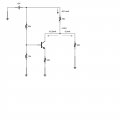
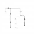
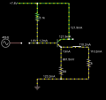
Common emitter npn Ib and Ic

Thread Starter

cmisip

Joined Sep 23, 2017
89
IR3 = IR5 + Ic

IR3 = VR3/R3

IR5 = VR5/R5

VR3 + VR5 = 20

IR5 + Ic = (20 - VR5)/R3

Ic = (20 - VR5)/R3 - VR5/R5 all values known to solve for VR5


With a bit of algebra ( If the above is correct, I'm a little rusty ), you can calculate VR3 and VR5 so it seems. I have to look into nodal analysis.

Thanks,
Chris
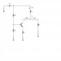
 

hobbyist

Joined Aug 10, 2008
892
The only thing I could think of is that R3 current is technically not Ic anymore because of the resistive load. Ic is only the positive current entering the collector terminal of the transistor and going towards the emitter.
You are correct on that, R3 carries both branch currents, the IC value plus the additional current through the load R5.
 

Thread Starter

cmisip

Joined Sep 23, 2017
89
It seems also that you should be able to adjust the value of quiescent Ic such that with a known load value, the collector voltage would stay at the value you predicted instead of sagging down.

Thanks,
Chris
 

hobbyist

Joined Aug 10, 2008
892
I know that would seem that way, but doing simulated experiments with varying resistances in parallel and a series resistance shows, that when one of the parallel resistances goes lower, the voltage will always drop.

The current through the other parallel resistor can be increased, by lowering it, but the total resistance has dropped lower thereby lowering the voltage.

So how is this remedied, if you have a DC coupled load in parallel with your transistor, as shown in your example, the only way to maintain the set voltage is to lower the collector resistor, this will then cause more current to be distributed to the load, thereby raising the voltage, across the parallel combination, of both the transistor and the load.

The reason for this is a transistor does not produce current, it only lowers its apparent resistance like a variable resistor, to allow more current to flow through it.

I could draw this up if you would like to see it in simulation form, it may be more helpful in understanding this.
 

Thread Starter

cmisip

Joined Sep 23, 2017
89
I would appreciate that. Could you post it in LTspice format? I would be able to play with the settings and see how it works.

Thanks,
Chris
 

hobbyist

Joined Aug 10, 2008
892
I don't have LT spice but you could copy these circuits.

DISCLAIMER: the following excersise is just an excersise it is not the way to design amplifying transistor circuits, mush more is involved in that! However this is just to teach how to work the problems in a logical manner of keeping the transistor in a quiescent state during different load changes.

Now this is just samples, to help better explain how to bias the transistor, it's up to you to to tweak values to get optimal performance.
This instruction, works only for DC loads as you are trying to match impedances as part of the biasing of the transistor stage itself.
But as you play around with this trying all kinds of values for the load, then trying to bias the transistor to work at a set voltage, you will be able to discern what values can be realized, and how much you can change values before the transistor cannot handle it linearly any more.

This should be a good excercise to learn the limits of transistor behaviour, and such.
Doing this exercise will give you a better understanding when you hear the phrase, "impedance matching", where you want the output impedance of a driver stage to be much lower than its load.

I'm assuming you have a good understanding of voltage and current dividers, ohms law, the basics because it only takes the basic theorems to design a transistor stage.

Start out by:
Choosing to set the collector voltage to (VCC / 2)

First you have a DC load of 2K ohms, so since you already have a collector resistor of 1K ohms, then you can set the voltage to VCC/2 by designing for the transistor branch to have close to the same amount of current as the load, so the parallel combination can equal close to the 1K ohms collector resistor. That would give 1/2 supply voltage at the collector.

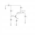
5 Ma.jpg


Now lets say your load is switched over to a smaller value, and as an exercise, you would like to bias the transistor stage to meet the demand of keeping quiescent voltage at the collector.

Alright here is what you do,

1). lower the collector resistor to 1/2 of the load value. (you can change it to any lower value you want)
2). Now just for starters to introduce some guidelines, (not the best for designing an amplifier),
change your emitter resistor to a realistic value, that is around half the load value. (1/2 load)
3). Now calculate the current through the load resistor then multiply that current times the emitter resistor so as to attain the emitter voltage.
4). add the vbe to that value to give you the voltage at the base.
from there use your knowledge of biasing the base divider to give you the current needed, so as to bias the transistor into its quiescent voltage at the collector that you were designing for.

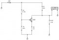
20 Ma.jpg


If your unfamiliar of how I got those resistor values than let us know, and we'll show you how to calculate those values.

This was just done in simulation so you should be able to use your simulator to experiment with differing load values.
Have fun.
 

Thread Starter

cmisip

Joined Sep 23, 2017
89
I have been doing some more simulations on this.

I originally thought that I would just raise the Qpoint up but then I realized the capacitor pulls it down to zero center anyway. So the solution that I thought of was to increase the voltage span by increasing the the collector resistance and hence the voltage gain which is curiously going opposite the solution you suggested. I used an online calculator for the rebiasing just to speed things up.

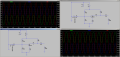
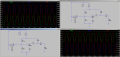
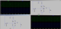
Here is the before. The right side is the original biasing and collector resistor value. The goal is to keep the collector voltage at 5V to -5V despite the load.

The left side is the rebiased version with increased collector resistor value. The left side has a voltage span of 6V to -6V. The right side (original) has a voltage span of 5V to -5V.

upload_2017-11-28_6-9-21.png

After the 50K load is connected. The one on the right side shows the collector voltage span being reduced to 4V to -4V. The one on the left that was rebiased to allow for a 6V to -6V voltage span, now shows 5V - -5V. The 50k resistance pulls the top down and the bottom up by about 1 volt. So the rebias seemed to keep the collector voltage at the desired 5V - -5V despite the load.

upload_2017-11-28_6-13-28.png

I have to try it with the technique you suggested to see if I come up with similar results.

Thanks,
Chris
 

hobbyist

Joined Aug 10, 2008
892
After you practice with the above tutorial (post#66) Here is the advanced tutorial that finally leads to a practice exercise in designing a DC amplifier using your learning of impedance matching, from the previous lesson. Enjoy.
----------------------------------------------------------------------------------------------------------
Now once you get a good handle on the first exercise, keeping the transistor above water during conflicting DC load changes, you can be ready for an advanced exercise in solving for biasing the transistor under conflicting load changes without changing the collector resistor. In the previous exercise you were given the option to change the RC value so as to make it match the parrallel combination of the transistor branch and the load branch, that way it ensures you have midrange on the bias of the transistor, all you needed to do was make both branch currents equal.

Now in this advanced exercise, keep the RC value constant, and change the DC load to differing values, and keep the transistor floating midrange as much as possible. You will soon discover that the currents will divide unequally through the transistor branch and load branch. This will teach you how to solve for the transistor current needed to match the load so as to keep the transistor output in its linear range. Again these exercises work only for DC coupling, your learning how to work the problem of biasing a transistor, with unusual load demands.

Here are the steps to bias the transistor.

We'll keep the RC value the same 250 ohms.
using the last example change the load to an unusual value as 17K ohms. (let's also assume you don't know what this load impedance is, it's in a black box. also theres no terminal leads to connect a meter to completely unacessible)

2.jpg


1). You first disconnect the transistor branch.
Now you have one series circuit with RC and the unknown Load.
Take a Voltage measurement across RC. and solve for current flowing through it.
Jot down this value.

2). Solve for the remaining voltage dropped across the Load, and using ohms law solve for the value of this Load resistance.
Now you have a Known resistive load to work with.

3). calculate the current that will flow through load when the voltage across it is your set voltage, this case (VCC / 2).

4). calculate the current that will flow through RC with the remaining voltage. again in this case (VCC / 2).

Now that determines the amount of current the Load needs in order for the set voltage to be dropped across it.

The value of current you calculated through RC with the new set voltage, is the total current it needs to drop its voltage according to your design requirement (set voltage).

5). take the RC current value (new set voltage) and subtract the (new set voltage) current flow through the Load, and this will give you the value of the remaining current that needs to be taken through the transistor, to bring the voltage across the load down to its new set value.

6). From there do your normal biasing techniques to supply this new calculated current through your transistor.


3.jpg


Now lets analyse this circuit you may be familiar with the terms used on this board about DC gain of the stage where (RC / RE)
The gain (DC) of this stage, is around (250/160) ~= 1.6 (Av) dc.
Not much of an amplifier.

But now that you know how to bias the transistor for differing loads, you can rearange the component values to get this to amplify some small signals.

Therefor, If the emitter resistor was changed to around 24 ohms then a dc gain of around 10 may be realized.

Again bias the transistor to keep around VCC/2 at its collector, with a 24 ohm emitter resistor,
So before applying a signal to this, check to see if the transistor Q point is around (VCC/2) {(always tweak resistor values if needed to get your design aim) I just used standard resistor values for ,RE, R1, R2 to get it close to Qpoint set voltage (VCC/2)}.

4.jpg

If it is, then this stage is ready for a test run to see if it can amplify a small AC signal.

5.jpg
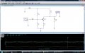
Vinput (bottom yellow) 200mV. pk-pk and the Vout (green) around 2V pk-pk

Now drop the load to around 300 ohms and redesign the stage.

This is the conclusion of these exercises for biasing for a DC load, practice this until your comfortable with calculating Gain and solving for resistor values to get you close to design goals.

Above all, have fun with it.
 
Last edited:

Thread Starter

cmisip

Joined Sep 23, 2017
89
Thank you very much for this. I have done the first exercise and it greatly improved my understanding of what is happening on that side of the circuit with a load.

What I have learned.
1. The collector resistor is in series with a parallel combination of Load resistor with the emitter leg of the the transistor.
2. If we want to maintain Vcc/2 at the collector, then the collector resistor must equal the parallel resistance combination so they both have equal voltage drops.
3. Now that we know how much current the load requires to stay at Vcc/2, we can plan for an equal value of Ic for biasing the base resistors.
4. The load current does not have any appreciable effect on Ic as it is defined as the positive current entering the transistor collector terminal. The load current does affect the current through the collector resistor.

I have yet to do the second set of exercises.

Some other implications I see at this point.

1. To maintain the collector voltage stable with a load, the load must not draw too much current. In fact if it draws very little then the collector current approaches the value of Ic and so the collector voltage remains stable.
2. If the collector resistance is very low with respect to the load, despite the increase in load current, there might not be a significant change in the voltage drop on the collector resistance resulting in a more stable collector voltage.

Thanks,
Chris
 

hobbyist

Joined Aug 10, 2008
892
Look at your first post in this thread and then reread this:

1. To maintain the collector voltage stable with a load, the load must not draw too much current. In fact if it draws very little then the collector current approaches the value of Ic and so the collector voltage remains stable.
2. If the collector resistance is very low with respect to the load, despite the increase in load current, there might not be a significant change in the voltage drop on the collector resistance resulting in a more stable collector voltage.
You have come a long way, what you wrote above is in essence, what transistor amplifier circuit design hinges on, it's all a matter of matching impedance requirements for each stage from input to output, while maintaining the integrity of the signal, with a final amplification.
 

Thread Starter

cmisip

Joined Sep 23, 2017
89
You have come a long way, what you wrote above is in essence, what transistor amplifier circuit design hinges on, it's all a matter of matching impedance requirements for each stage from input to output, while maintaining the integrity of the signal, with a final amplification.
I took you guys for a rollercoaster ride :) Thanks for sticking around.

I have completed the second exercise.

STEP 1. Starting with NO LOAD, I calculated the resistor values as follows, given RC of 250.

1. Select an emitter resistor that is 1/10th of the collector resistor.

Re = 25 R

2. Calculate Icmax which is when Vce resistance is the least, leading to a .2 volt drop across Vce. The collector loop then becomes

Icmax = 10 / ( 250 + 25 )
= 0.036363636363636364

3. The current at Vcc/2 is half and Ibq would be 100 times less

Icq = 0.018181818181818182
Ibq = 0.000181818181818182

4. The emitter current when the hfe is 100 is
Ie = Icq + Ib
= 0.018181818181818182 + 0.000181818181818182
= 0.018363636181818182

5. At Q point, the emitter voltage would be
Ve = 0.018363636181818182 * 25
= 0.459090904545454545

6. Calculate the base divider bias
R2 = VR2 / 10 * Ib
= ( Ve + Vbe ) / ( 10 * Ib )
= ( 0.459090904545454545 + .63 ) / ( 10 * 0.000181818181818182 )
= 1.089090904545454545 / ( 10 * 0.000181818181818182 )
= 599

R1 = VR1 / ( 11 * Ib)
= ( Vcc - VR2 ) / ( 11 * Ib )
= ( 10 - 1.089090904545454545) / ( 11 * 0.000181818181818182 )
= 4455.45

Resulting Qpoint is 5.918 volts.

QUESTION: Is this the correct way to do this? On the LTSpice simulation I got a simulated Ic of 16.331 mA instead of 18.18 mA.

I am going to go with the simulated IcQ for the next calculations.

STEP 2: Add a 17K LOAD. This causes Collector voltage to go down to 5.8327 volts. The goal is to restore the collector voltage to 5.918 volts.

The parallel resistance of 17k + 25 is 24.96 volts.

At 5.918 volts, RL requires 5.918/17000 = 0.000348117647058824 A to remain at this voltage.

Therefore IRc must increase by this much.
IRC = Ic + 0.000348117647058824
= 0.016331 + 0.000348117647058824
= 0.016679117647058824

To increase IRc to this new value, we need to reduce the collector resistance.
RC = VRC / 0.016679117647058824
= (10 - 5.918) / 0.016679117647058824
= 244.74

Changing RC to 244.74 raises the collector to 6.00 volts with NO LOAD.
When the 17k load is connected, the collector voltage reduces to 5.91 volts.

Therefore, reducing the collector resistor allows us to increase the collector current to account for the current use of the load. This keeps the voltage at the collector from sagging.

Implications:
1. Ic does not seem to change with the addition of the Load. The quiescent Ic will be the same so no rebiasing is necessary. However, the collector resistor must be reduced to meet the increased RC current needed.
2. Past a certain increasing value of RL, the parallel resistance combination does not change in any significant way so higher resistive loads don't change the collector voltage anymore. It remains stable with the load.

upload_2017-12-2_15-38-50.png

Thanks,
Chris
 

hobbyist

Joined Aug 10, 2008
892
It looks from your calculation math you have a good handle on biasing for Qpoint.
However as I was reading your procedures for lesson 2, I think you missed the whole point of the lesson.

You demonstrated you can bias the stage, then add a load, higher than the output resistance, and learned there is minimal effect on high load with respect to Zout. Which is essential to learn that.

However I think you missed the whole point of lesson 2, I was trying to point out that there are times in a design, where you may not have a known value of load resistance, this is very important:

Example: on my simulator, I had the ability to change the load resistance without looking at it, and not have it show on the screen, then through measurement techniques determined the load value, and biased the stage, (to provide any reasonable output voltage I desired.).

If you follow each of the steps in lesson 2 you will be able to approach the design for how to determine the amount of current your transistor needs to take across a DC load to keep a set voltage at its output. (any realizable voltage you choose to design it for).

This is very important because there are times you may not need a amplifier, but a voltage reference source or current source, and you have to be able to design the output of your transistor to supply the necessary current or voltage, to meet a requirement.

Lesson 2 was given to work you through the exercise of putting any reasonable value of output voltage across a DC load, by determining the currents through the load and through the transistor branches to make it possible.

I see your eager to learn this, so since I am always at the basic level in transistor circuit design, I like to help those who are just starting out.

I'm going to work out an example of a DC transistor amplifier, where I'll use 3 transistors coupled together, and it will be a good example to show how the output voltages of the first 2 transistor stages are not mid load line at all, but at a set voltage to meet design requirements.
If you don't mind I'll post it in this thread for you to look over it.

Again, you did an excellent job in biasing your transistor, and then add a load, now its time to work from the output side where a load is already present, (as usually the case in design work) and you have to design the stage to drive it.
 

Thread Starter

cmisip

Joined Sep 23, 2017
89
Example: on my simulator, I had the ability to change the load resistance without looking at it, and not have it show on the screen, then through measurement techniques determined the load value, and biased the stage, (to provide any reasonable output voltage I desired.)
I missed that one. I wondered why I needed to do any measurements. I dont seem to have that functionality in LTspice. Components need to be specified and then measurements of currents and voltage can be taken.

I also thought this was about amplification of an AC. But I have been wondering how I might use a transistor as a fixed current source or voltage source.

I think I missed another part of the lesson. What if the collector resistor cant be changed? In that case, the load current must be pulled from Ic. In which case, rebiasing would be necessary with a new Ic value. I have to check that out.

Please go ahead and post your transistor design. All these help further my understanding.

Its really hard and slow typing with a stylus on a tablet. Please excuse my lack of verbosity.

Thanks,
Chris
 

hobbyist

Joined Aug 10, 2008
892
That's OK Chris, no problem, I'm working on the next lesson, that will show how to design for DC coupling, between stages to bring input impedances up, so as to drive loads, that normally couldn't be driven under normal CE amplifying stages.

This will than introduce you to AC coupling so when its all put together you can use the DC coupling stages for increasing input impedance, and the AC stage can be a normal CE stage for the amplification.

However before I post it, I'm going to build it actual (breadboard), and test it out to make sure it's not just a theoretical design, but an actual working design.

Stay tuned.
 

hobbyist

Joined Aug 10, 2008
892
I had too many pics to be able to upload to this thread, didn't want to overcroud your original thread, so here is the completed lesson #3 which I promised, it's in my blog.

click on the links below.

part1 is the excersise, part2 are some actual real oscilloscope waveforms of the completed project on a real breadboard.


Lesson #3

https://forum.allaboutcircuits.com/...biasing-for-designing-amplifiers-part-1.1164/


lesson #3 continued (with actual circuit (non simulated) waveforms.)

https://forum.allaboutcircuits.com/blog/leson-3-transistor-biasing-for-designing-amps-part-2.1165/


----------------------------------------------------------------------------------------------------
 

Thread Starter

cmisip

Joined Sep 23, 2017
89
Thank you for putting this together. There are a lot of lessons here. I will try to start with understanding the circuit design. It will take me several postings to fully appreciate all the information here.


The ultimate goal I think is to be able to match the output impedance of the Q3 CE amplifier which is its RC resistor (33k) with the CC stage that follows it. The input impedance of the CC stage must therefore amount to ~33k. Starting from the 8 ohm speaker, if there is an AC signal, the capacitor is shorted so the 8 ohm and 68 ohm speaker would be in parallel for roughly 8 ohm equivalent value. For a CC, the input impedance is ~B*RE so it would be 8 * 100 or 800 ohms.


The next stage Q2 CC amplifer is confusing me a bit. The 1.6k resistor will be in series with the 800 ohms input impedance of the Q1 CC stage. This would give a total of 1600+800 = 2400 ohms. Multiply that by 100 to get 24000 ohms. It seems short of 33k needed. If the capacitor shorts out the 1.6k resistor when there is an AC signal, then its effectively zero ohms and the emitter resistance would just be 800 ohms and multiplied by 100 will just be 8k. This leads to a bigger discrepancy between CE output impedance and CC input impedance ( 33k ↔ 8k ).


QUESTION1: Can you explain how the 33k ohm input impedance was achieved? Does the input impedance of the CC stage really reduce to 8k with AC signal? If it does, wouldn’t this impedance mismatch cause poor power transfer from CE to CC stage when the amplifier is being used?

--------------------------------------------------------------------------------------------------------------------------------------------------------------------------------------

Q1 CC:


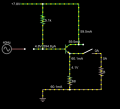
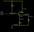
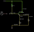
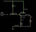
With no LOAD, this puts the voltage across the Q1 CC base to emitter to ground at V=IR, V= .0005948*101*68=4.1 volts. This can be roughly arrived at by using a voltage divider formula with a 5100 resistor and a 6800 resistor. The base current would be (7.8 -.7 ) / (5100 + 6800) = 596.63 uA.


With LOAD, the parallel resistance is 7.16 ohms. The voltages would divide according to component resistors 5100 and (7.16 * 101) = 723 which will put .968 volts aross the 723 ohm resistor. The base current would be (7.8 -.7 ) / (5100 + 723) = 1.2193 mA.


The above solidifies the idea that looking from the base towards the emitter, the emitter resistor looks like it is RE * Beta.


This in turn allows us to calculate the power dissipation because the Vce voltage would be 7.82 – 4.09 = 3.73 Volts with NO LOAD and 7.82 - .968 = 6.85 volts with LOAD. Power dissipation would be :


3.73 * .0595 = 0.221935 Watts or 221.9 milliWatts with NO LOAD.


6.85 * .1219 = 0.8352588 Watts or 835 milliWatts with LOAD. If this is correct, the current setup would exceed the power rating of the transistor.


QUESTION2: Where did I make a mistake on the power calculation?
upload_2017-12-10_16-14-47.png

upload_2017-12-10_16-14-33.png

-----------------------------------------------------------------------------------------------------------------------------------------------------------------------------
Q2 CC:


Q2 CC thinks the entirety of Q1 CC is represented by a single resistor with input impedance of 800 ohms. A CC stage expresses the output AC signal across its emitter resistor (emitter to ground) and receives the input AC across its base to emitter resistor to ground. So the two can be directly connected provided that the biasing requirements of the following CC stage is met. For this scenario, Q2 CC must supply 594.9 uA at 4.8 volts in order to satisfy the biasing requirement. It will be then equivalent to the 5.1 k base resistor that it replaces.


QUESTION3: Do I need to worry about the previous CC stage's output impedance? It's a CC stage so it should be low. Do I worry about matching the previous CC output impedance with the following CC input impedance?

Please ignore the attached files. Don't know how they got there.

Thanks,
Chris
 

Attachments

Last edited:

Audioguru

Joined Dec 20, 2007
11,248
You show an 8 ohm load. Then are you trying to make an audio amplifier that drives an 8 ohm speaker?
Not this way because it puts DC in the speaker which might melt it and it causes its cone to move to one side all the time.

Your common collector (emitter follower) single transistor is a class-A heater. Most audio amplifiers use two emitter follower output transistors, an NPN and a PNP so that the PNP pushes the output negative and the NPN pulls the output positive called push-pull. They always have a small bias current and operate in class-AB. They either have a dual-polarity power supply so that the average DC output is 0V across the speaker or they have an output coupling capacitor feeding the speaker with signal but blocking any DC.
With negative feedback the output impedance of an audio amplifier is extremely low, about 0.04 ohms or less so that it damps the resonances of the speaker. The output impedance of an audio amplifier is never matched to the speaker and most amplifier stages also are not matched and have a low impedance driving a high impedance so that output voltage swing is not reduced.

In your last question #3 why do you wrongly talk of a CC driving a CC? It should be a CE driving a CC.
 

Thread Starter

cmisip

Joined Sep 23, 2017
89
@Audioguru

Hobbyist posted a design for an amplifier. I am trying to understand the design decisions. The design showed two stages of CC between the CE and the speaker.

The link is here:


https://forum.allaboutcircuits.com/...biasing-for-designing-amplifiers-part-1.1164/

The switch in the schematic I posted is supposed to be a capacitor. I just wanted to be able short and open the capacitor because AC shorts the capacitor. The capacitor should remove all the DC bias before it gets to the speaker. I just was trying to analyze the changes in voltages and current when there is DC only and when there is AC superimposed.

Thanks,
Chris
 

hobbyist

Joined Aug 10, 2008
892
The next stage Q2 CC amplifer is confusing me a bit.
Hi,
Yes I will get back with you on this, I need to go back over my design notes to recall the choices I made during the design.
Plus I want to study your observations from your above experiments, to see how everything worked out for you with it.
 

hobbyist

Joined Aug 10, 2008
892
Ok, I'm going to explain how I got my values, so you can use these steps as basic building blocks for you to improve upon that fits your design goals.

To solve for Q1 stage, I want around 400mW. diss. in Q1. (P / VCE ) = ICQ1
I considered Q1 sat. to be around 0.2V. so I take (Vcc - Vcesat) ~=7.8V.
I want 1/2Vcc to be across RE so (7.8V - 4V) = VCE = 3.8V.
Therefor (ICQ1= (P / VCE) = (400mW / 3.8V) = ~=105mA.

Of that total current I want the DC bias current to be 1.3 - 1.5 times greater than the pk-pk AC current through the load.
So I chose to use around 1.3 times greater therefor writing up equations,
{IC = (IE + IL)} and {(IE = (1.3 x IL)} rearanging gives { (IL = IC / 2.3) }.
so load current pk-pk =~45.6mA, which leaves around 59.3mA dc bias through REQ1 which also is ICQ.
Now REQ1=( 1/2vcc / IE) =~68 ohms.
I assume Beta =~100 for calcualtion purposes.
So the base bias resistor is calculated as follows,
VRBQ1 = (VCC - Vbe - VREQ1) = (8v - .7v - 4v) = 3.3V
IBQ1 = (ICQ1 / B) = (59mA / 100) = 590uA
and RBQ1 = (VRBQ1 / IBQ1) = ~5.59K ohms I went with 5.6K and the voltage was a little off so I chose to tweek it to a lower nearest value of 5.1K ohms.
So that establishes biasing the CC stage (Q1) for a chosen ICQ current.:

Now always build the stage and check voltages and tweek values as necessary.

OK now I chose to add another CC stage to up the Zin further yet.

Here is how I calculated the values:
.
CC stage Q2 needs to take the place of 5.1K ohm base resistor.
I know calculationwise I want to keep around 590-600uA flowing through Q2 to keep voltages proper at REQ1.
Therefore I chose an emitter resistor 1.6K ohms.
First why choose a emitter resistor, If I don't use an emitter resistor I don't have a easy way to establish a calculated current, the emitter resistor in combination with a voltage divider base bias network, always allow me to establish the current I want flowing through the transistor to a close approximation. In this case I need to set up this Q2 network to act as a current source to bias the Q1 stage, so I need some pretty accurate approximations, the emitter resistor makes that possible.

Now why the value of 1.6K ohms, because I want to put a voltage across Q2 to keep it in its linear region, so I chose to drop around 1V across the emitter resistor, and the remaining 2.3V to be VCEQ2.

Now the 2 base resistors for the base voltage divider of Q2 is calculated as I want the current through the top (supply) base resistor of Q2 to have around 1/10th of the collector current of Q2. And the base current IBQ2 =~ (ICQ2 / 100).

Therefor IBQ2 = 5.9uA. And current through pull up base resistor of Q2 = 59uA.

VBQ2 = (4v + .7v + VREQ2 + .7V) =~6.4V where VREQ2 =1v.
So pull down base resitor is calculated as (VBQ2 / (59uA - 5.9uA) ~=120K ohms.
and pull up resistor would be{ (VCC - VBQ2) / 59uA} ~=27K ohms.

DON'T MISS THIS:
MY calculated values are just ballpark figures, after I built this stage and tested it, I had to tweek values, until I was getting proper voltages where I needed them. I was more interested in raising the Zin so I worked in the direction of raising the base resistors, until I got proper voltage values without loading the divider.
That's why the 160K ohms for the pull down resistor.
and 33K ohms for the pull up resistor.

That's how the 33K ohms came about.

Now your question was, why use the 33K ohms for the Zout of Q3, when the Zin is low by way of the 1.6K ohm emitter resistor bypassed with a cap.

I chose to keep the 33K ohm resistor in place, to design the next stage, mainly because I didn't fell like going through the whole process of matching impedances and recalculating and such, however YOU ARE RIGHT, I should have matched the impedances better, you caught that very well, so see you are getting a good understanding of impedance matching stages.

Now as far as determining currents and voltages and such for Q3, I think I went through the whole process of calculating for quiescent values in the earlier lessons, post #66 and #68.
however, if any questions though feel free to ask, and I'll try to answer them.


I will look over your post above and answer the questions next post.
 
Last edited:
Top