Facebook
 Google
 GitHub
 Linkedin
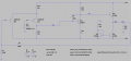
Which criteria should be used to choose R7 and R8 values? I've seen 150ohm in other similar circuits... There isn't a formula to choose them, right?
Do you think it's possible to have 0 DC at the input, so that I don't have to use C3?
Thanks
Do you think it's possible to have 0 DC at the input, so that I don't have to use C3?
Thanks