PCB layout for oscillator - separated GND plane confusion

Thread Starter

freeflyer

Joined Sep 9, 2016
148
I am designing a 4 layer PCB which uses an STM32L433 and working on the layout for the LSE and HSE crystals.

I referred to the application note AN2867 for guidance, but I am confused by the isolated ground plane underneath the crystals as shown in Figure 14...

1770127827400.png

https://www.st.com/resource/en/appl...als-and-stm32-mcusmpus-stmicroelectronics.pdf

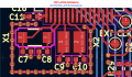
The layout is shown in the screenshots below and include:

  1. Isolated plane under the crystals on inner layer 1 and 2
    1. Note that both inner layer 1 and 2 are ground planes
      1. Inner layer 1 is continuous ground plane
      2. Inner layer 2 has some power tracks within the ground plane
  2. Connected isolated ground plane to pin 12 (GND) of STM32
    1. Pin 12 is VSSA (analogue ground), will this be a problem ?
    2. The STM32L433 only has a single ground pin (18)
  3. No tracks run under the crystals


1770127876626.png


1770127906575.png


1770127921071.png

1770127940017.png

1770127950005.png

I have designed a few boards using this STM32 device and did not use isolated planes under the crystals or a guard rail, but it still worked. Even the ST Nucleo development board for this MCU does not use a guard rail.

So should I continue with these isolated planes and guard rail or is there a risk it could cause issues ?

I dont know whether I should just design it the way I have previously, I would be furious if I spent a few hundred pounds on PCB fabrication and assembly only to find out that the crystals don't work due to the isolated planes and guard rail.

But the guidelines recommend this layout, so I am trying to do it correctly especially if it helps with EMI.

Below is an example how I previously designed the layout for the crystals....


1770127990489.png
 

Attachments

bertus

Joined Apr 5, 2008
22,909
Hello,

Your images do not show.
They are hosted on an other site that does not allow posting over here.
Upload the images to this forum to show them.

Bertus
 

MrChips

Joined Oct 2, 2009
34,698
I think all those vias is overkill. You can eliminate all the vias if the guard rail is connected to GND.
I think the main issues are:
1) Keep all traces short and straight and close to the MCU.
2) Keep the capacitors close to the crystal.
3) Connect the capacitors to the ground plane.

I don't see any problems with your layout except that the guard rail should also run in between the two oscillator circuits.
 

ronsimpson

Joined Oct 7, 2019
4,661
Looks good.
guard rail should also run in between the two oscillator circuits.
1) Keep all traces short and straight and close to the MCU.
I drew traces in blue, so it is easy to see. I just want to show that a trace does not have to enter a pad in the middle. It can enter any there you want then to then go to the center of the pad to "connect".
1770133191511.png
 

NewbDa

Joined Jan 21, 2020
13
If you closely inspect the guardrail design implemented in the application note, you’ll see that it clearly separates the LSE and HSE. Your design, however, does not. You can either follow exactly what the application note describes or use the diagram/picture that ronsimpson uploaded as he suggested.

Edit-1: What is the value of the HSE used by you in your previous STM32 designs? And, what is the value of HSE for your current design?
 

Thread Starter

freeflyer

Joined Sep 9, 2016
148
If you closely inspect the guardrail design implemented in the application note, you’ll see that it clearly separates the LSE and HSE. Your design, however, does not. You can either follow exactly what the application note describes or use the diagram/picture that ronsimpson uploaded as he suggested.

Edit-1: What is the value of the HSE used by you in your previous STM32 designs? And, what is the value of HSE for your current design?
Thanks, I will implement the guard rail between the two crystals.

The HSE is not actually used, its there just in case the MSI (multi speed internal) RC oscillator has too much drift etc. If it is used, the frequency will be 12.288MHz as it will be used to clock I2S audio data. But at the moment the MSI seems to work.
 

du00000001

Joined Nov 10, 2020
189
The GND "island" should extend underneath the X* pins!

The intention of this setup is to shield the clock signals (especially XI*) from EM interference. Thus the guard ring should also encircle the X* pins (provided you can have a trace between 2 pins). Having only a single GND pin in the mcu can be considered some kind of design flaw - usually there is a GND pin next to the X* pins available. The vias between the guard ring and the GND island are basically OK - half the number might do as well.
Whether extending the guard ring between MSE and HSE is really required depends: if the two inner pins are both XO* (way less susceptible for EMI) you can go without. If they are XI* (or a mix of XI and XO), I'd consider this another design flaw and would try to route the guard ring inbetween (and also between the pins).
 

Thread Starter

freeflyer

Joined Sep 9, 2016
148
I have modified the design as shown in the screenshots below. The modifications include:

  • GND taken from pin 63
  • Seperate isolated GND planes for both crystals X1 and X2
  • Extended isolated GND plane to go under the STM32 pins
  • Guard rail inbetween both crystals
    • Does this part of the guard rail need vias and if so, which isolated plane would they connect to ?
  • Reduced via spacing on guard rail


Im still unsure about this design, there is already one issue because the isolated GND plane for X2 has no connection to GND so Im unsure how to resolve this.

1770580190541.png


1770580205306.png

1770580218731.png

1770580230996.png
 

du00000001

Joined Nov 10, 2020
189
No need to split the GND underneath the 2 oscillators. As no GND pin is really close to the X* pins, I'd connect the island to the "global GND" with a trace underneath the middle between pins 4 and 5.
After joining the 2 "islands" you can also have the space for vias connecting the "dividing trace" on top to GND. (And yes - such vias are recommended.)
BTW: make sure the guard ring is covered by the GND island everywhere! (Currently I can see a short piece of track (close to the lettering "C9") that runs partly above the gap around the GND island.)
 

MrChips

Joined Oct 2, 2009
34,698
I don’t see any advantage of having vias to GND at the capacitors and at the guard ring so close to each other. I would eliminate four vias and replace it with one via. Put a trace between the GND of the two capacitors and join to the guard ring.

Remove most of the bends going to the xtals.
 

Thread Starter

freeflyer

Joined Sep 9, 2016
148
I don’t see any advantage of having vias to GND at the capacitors and at the guard ring so close to each other. I would eliminate four vias and replace it with one via. Put a trace between the GND of the two capacitors and join to the guard ring.

Remove most of the bends going to the xtals.
Thanks, so like this then ?

1770633483669.png
 
Last edited:

Thread Starter

freeflyer

Joined Sep 9, 2016
148
Looking better.
You have two vias to GND close to the capacitors. Why not consolidate the two into one via like this?
Thanks, like this ?

Also, does the gap around the isolated GND plane matter (currently 0.2mm) ?

And does the width of the GND track matter, which connects the isolated GND plane to the main GND plane i.e. the blue track on bottom layer (currently 0.5mm) ?

1770651855627.png
 

MrChips

Joined Oct 2, 2009
34,698
A guard ring is usually employed to prevent leakage current between components and traces. The capacitance effect of a guard ring can influence performance especially at very high frequencies. No current is expected to flow into the guard ring.

In my opinion, the use of that many vias between the guard ring and the ground plane is excessive. Also, I don't see any advantage of having an isolated GND plane in this application. Keep in mind that the oscillator frequencies for this MCU are typically 32 kHz and 8 MHz. These are relative low frequencies where PCB layout is concerned.

The most important PCB layout practices are:

  1. keeping distances between MCU, xtal and capacitors as short as possible
  2. short and straight tracks between MCU, xtal, capacitors and GND
  3. GND plane on the bottom side

I have laid out many PCBs for STM32 and have not experienced any issues related to xtal clock performance. I have never employed a guard ring around the xtal oscillator.
 

Thread Starter

freeflyer

Joined Sep 9, 2016
148
A guard ring is usually employed to prevent leakage current between components and traces. The capacitance effect of a guard ring can influence performance especially at very high frequencies. No current is expected to flow into the guard ring.

In my opinion, the use of that many vias between the guard ring and the ground plane is excessive. Also, I don't see any advantage of having an isolated GND plane in this application. Keep in mind that the oscillator frequencies for this MCU are typically 32 kHz and 8 MHz. These are relative low frequencies where PCB layout is concerned.

The most important PCB layout practices are:

  1. keeping distances between MCU, xtal and capacitors as short as possible
  2. short and straight tracks between MCU, xtal, capacitors and GND
  3. GND plane on the bottom side

I have laid out many PCBs for STM32 and have not experienced any issues related to xtal clock performance. I have never employed a guard ring around the xtal oscillator.
I am using 32Khz for LSE and 12.288MHz for HSE, so are you saying I don't need to bother with isolated GND planes and guard rail ?
 
Top