Just some general questions about remaking something from the past

Status
Not open for further replies.

Audioguru

Joined Dec 20, 2007
11,248
Yes. And in an earlier post it was just fine, what changed?
The supply was 16V in post #305. Now you have the TDA7396 bridged amplifier using the absolute maximum supply of 18V which produces a little more power and a lot more heat.

If you look at AG's post #318 now all of a sudden it's 27W or 40W. If you use that formula "which I know is correct" then the actual watts are 6.65W with 18V
Its datasheet shows a graph of power into a 4 ohm speaker vs supply voltage. When the distortion is 1% (many people can hear it) the power is 27W and with 18V the power is about - (dangerous, they do not show it), I guess about 32W. Then if it is not bridged its output power with an 18V supply is 32/3.5= 9.1W with 1% distortion or about 7W with low distortion.
Don't forget that a bridged amplifier almost doubles the voltage swing across a speaker which almost doubles the current in it. Then double-double= 4 times but more voltage losses reduce the increase in power to about 3.5 times.

27W with 1% distortion is about 25W with low distortion. An ordinary car radio produces about 15W with low distortion and 30W sounds only a little louder. Here you will have 25W which will sound a little less than a little louder. Is it worth doing?
The datasheet for the TDA7396 shows all its spec's with a 14.4V charging car battery, not 18V. The graph stops at 16V. Then with your 18V boosted voltage it will roast itself to death soon. Bad idea.
 

Thread Starter

Berzerker

Joined Jul 29, 2018
623
Thank you AG I wasn't going to put 18V to it maybe around 14V to 16V. It's just a project (?) I just want to see if I can do it. I will have design something I've always wanted to do and have ( with a lot of help). around $50 bucks each to make.
 

Thread Starter

Berzerker

Joined Jul 29, 2018
623
Diptrace question.
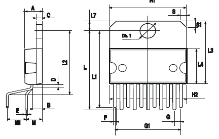
I look at the datasheet and the space between the leads on a capacitor is 2.5mm. I want to put one in my schematic with these dimensions.
But diptrace has these messed up numbers and nowhere I look do I see 2.5mm. How do you turn on dimensions in diptrace to where you see what the lead dimensions are? If you want to edit one to your dimensions you have to click and just see if one is close. I noticed some have the dimensions in the editor some don't. I guess what I'm asking is like in AutoCad how do you show dimensions to anything in diptrace.
Edit: My post #313 I made a pattern but when it shows up in the schematic it doesn't show the pin layout till I hover over it. can I change this?
Edit 2: got how you place dimensions finally
Edit 3: Snap is everything
 
Last edited:

Thread Starter

Berzerker

Joined Jul 29, 2018
623
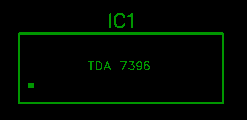
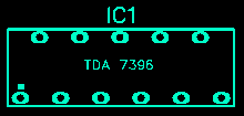
No ebeowulf I got the pins and numbers attached to the component correctly. Shows up in the component editor fine, all lines show them going to the correct pins. I open the PCB layout and place my part in and only the outline, pin one orientation mark and part name show up.

Then when I hover over it the pins show up (?) Just wondering was this normal?
 

ebeowulf17

Joined Aug 12, 2014
3,307
No ebeowulf I got the pins and numbers attached to the component correctly. Shows up in the component editor fine, all lines show them going to the correct pins. I open the PCB layout and place my part in and only the outline, pin one orientation mark and part name show up.

Then when I hover over it the pins show up (?) Just wondering was this normal?
Are you talking about the holes and pads? Is your copper layer turned off? Or maybe pads are turned off in the objects tab?

I don't know - I can't replicate what you're describing. Depending on my settings, pads and holes are either visible or not, but they never appear only when I hover nearby.

Does this happen on other components that already existed in the stock libraries, or only on the one you created?
 

Thread Starter

Berzerker

Joined Jul 29, 2018
623
Only the one I created. I'll check the copper layer. And another question the pins are actually rectangle .022 in. x .032 in.
I can only find how to make them oval or square or rectangle. But nowhere have I found to set this size in the pin manager or pad properties.
 

shortbus

Joined Sep 30, 2009
10,049
I look at the datasheet and the space between the leads on a capacitor is 2.5mm. I want to put one in my schematic with these dimensions.
Which screen are you using? There are two, one in inches and one in metric. So if you are using the inch one you need to convert your metric dimensions into inches.

Only the one I created. I'll check the copper layer. And another question the pins are actually rectangle .022 in. x .032 in.
I can only find how to make them oval or square or rectangle. But nowhere have I found to set this size in the pin manager or pad properties.
This is why I do it the way I described earlier and pick a component that already has the configuration and modify the pins names.
 

Thread Starter

Berzerker

Joined Jul 29, 2018
623
Sorry shortbus I'm back on the IC. I made a mistake on the layout and size and went to correct it. I was assuming that if you made a component up only those values width, height, length were in that editor. It looks like the pattern for the PCB not the IC itself.
https://www.mouser.com/datasheet/2/389/tda7396-957244.pdf
The pins still don't show up in the PCB layout " working on it" I'll figure it out eventually.
let me explain: I made an IC up, created the pattern, attached the pattern to the IC everything there is great. all lines, names, etc. go to the correct thing. I insert it into the PCB layout and only the outline shows up as above. Only when I hover over it do the pins show up. Still looking for how you tell the component editor the size of the pins, I found length.
shortbus said:
This is why I do it the way I described earlier and pick a component that already has the configuration and modify the pins names.
You actually would have been proud of me I actually done great free handed.
and I merged my layers before I hit save.
 
Last edited:

ebeowulf17

Joined Aug 12, 2014
3,307
I merged my layers before I hit save.
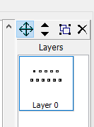
Not sure what you mean by that, but it may have been a bad idea... the resulting pattern needs to have separate layers in order for drill holes, copper pads, solder mask openings, and silk screen markings to all work properly. If all of that gets smashed into one layer, you won't get useful board layers out of your PCB layout when it's done.
 

Thread Starter

Berzerker

Joined Jul 29, 2018
623

I merged the layers in the pattern editor to make it one layer. I thought that's what you were suppose to do(?) I might have messed up and need to start all over.

Now I got this little cross mark at the bottom left and can't get rid of it and it shows up in the PCB layout.
 
Last edited:

Ylee5763

Joined Sep 23, 2015
27
Ok I found an old set of Mindblower Speakers in a box cleaning out a room. I'm pretty sure they no loner work. But it got me thinking could I resurrect these, create my own company and start manufacturing them. The company was called Tenna they were around in the late 70's and early 80's and as far as I know they no longer exist. Spent most of the day yesterday drawing it out on the computer, circuit board, components and looking up what they were called. I know nothing about electronics as I was machinist all my life with a little study in mechanical design and using CAD. They are mostly rusted and the parts have no clear markings on them! If they (Tenna) are no longer in operation can I re-do them and sell them without like copy right infringement, name infringement...etc? I would be making upgrades to the old design as they were notorious for failing after about a year with the PCB board being the worse about burning out the embedded wiring between components. But I have a few question I don't know how to get the answers too.

Without the Markings (numbers and ID's) how do you tell what they were?
And if I need to put a meter on them is there a chart that can tell me input, output voltage, ohms or whatever it's call to identify what they are.
I not trying to get you guys to do my work for me just point me in the right direction.
The unit consists of only a few parts;
1. (1) PCB board
2. (1) Transformer
3. (2) Diodes
4. (2) Capacitors, One being a ZSF the other same kind only larger
5. (2) Transistors
6. (1) Coil, I know it's function was to change it from a three wire output to a two wire output cos the first ones hooked up to special speaker with a double coil. Later models used this because the three wire speaker became hard to find or became too expensive and the coil was cheaper and you could now use any speaker on the market.
Any help or feed back would be appreciated!
 

Ylee5763

Joined Sep 23, 2015
27
the hardest parts to figure out are the transformer and coil if you are not familiar with transformer design. They are critical parts for this application.
 

Thread Starter

Berzerker

Joined Jul 29, 2018
623
Ylee5763 said:
the hardest parts to figure out are the transformer and coil if you are not familiar with transformer design. They are critical parts for this application.
Yea I kinda figured that out the hard way. Haven't gave up on the original design but I had to put it on the back burner till I find more info on them.
 

shortbus

Joined Sep 30, 2009
10,049
I merged the layers in the pattern editor to make it one layer. I thought that's what you were suppose to do(?) I might have messed up and need to start all over.

Now I got this little cross mark at the bottom left and can't get rid of it and it shows up in the PCB layout.
I didn't look at your real component. But if you changed a 'SIP"(single inline package) into a "DIP"(dual inline package) and the part doesn't come in DIP how will it fit your board? Also never saw a part in DIP that didn't have the same number of pins on both sides, with the unused ones marked something like "NC"(no connection).
 

Thread Starter

Berzerker

Joined Jul 29, 2018
623
Maybe I still don't understand shortbus (?). The transistor only has 11 pins. 6 on one side 5 on the other. I thought it was kinda like AutoCad and you made your component up just like it would be before you solder it to the board.
https://www.mouser.com/datasheet/2/389/tda7396-957244.pdf
I thought the pattern was the spacings on the pins so as you place the component in the PCB layout it was to the dimensions of the transistor.
I placed the pins all in-line in the component editor because that's how they are on the transistor.

I have a .eli and a .lib in my folder. No sip or dip
 
Last edited:

ebeowulf17

Joined Aug 12, 2014
3,307
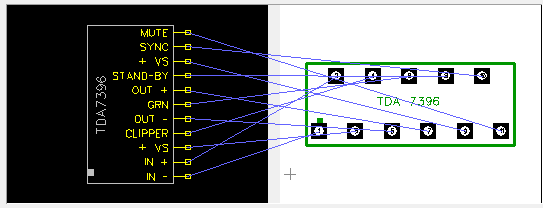
In the component editor, you can arrange pins any way you want. It quite often is useful to arrange them in ways that are nothing at all like the physical arrangement... maybe putting power on top, ground on bottom, signal in on left, and signal out on right, just as one possibility. Look at schematic symbols for op amps, logic gates, or microcontrollers as examples. They rarely relate to the physical configuration.

So, if you're happy with them as they are, that's fine. There's no need for them to be in two rows like the board holes... but there's also no need to put them in a row at all. The goal on the component layout should be to make the clearest, most logical, most readable, most intuitive schematic you can.

The fact that your pins only appear during mouse hover is disconcerting. Not sure what to make of that. There are two types of layers involved here. I don't think collapsing drawing layers like you showed earlier should affect which board layers various things are on (copper, solder mask, etc,) but I'm not totally sure either way. I'll have to test it, but haven't had time yet.
 

Thread Starter

Berzerker

Joined Jul 29, 2018
623
ebeowulf said:
n the component editor, you can arrange pins any way you want. It quite often is useful to arrange them in ways that are nothing at all like the physical arrangement... maybe putting power on top, ground on bottom, signal in on left, and signal out on right, just as one possibility. Look at schematic symbols for op amps, logic gates, or microcontrollers as examples. They rarely relate to the physical configuration.
Great then I don't have to re-do it.
ebeowulf said:
The fact that your pins only appear during mouse hover is disconcerting. Not sure what to make of that. There are two types of layers involved here. I don't think collapsing drawing layers like you showed earlier should affect which board layers various things are on (copper, solder mask, etc,) but I'm not totally sure either way. I'll have to test it, but haven't had time yet.
I deleted the pattern and done it all again and didn't merge the layers and the pins still don't show up till I hover over them. Got this on my list for today to look up.
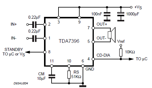
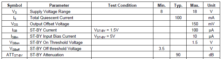
My next problem is the schematic and trying to understand what they mean with the stand-by voltage.
Datasheet: https://www.mouser.com/datasheet/2/389/tda7396-957244.pdf


Looking at the diagram it shows the arrow pointing "out" from the stand-by pin (#8), if you read the datasheet it says stand-by voltage is 1.5 to 5V. When I connect 5V to it in the schematic it's an error. leave it unhooked and no errors. Clipper pin (#4) also shows an arrow out. I assume this would go to some sort of LED or component to indicate there is a fault. But scroll down and it also shows 5V (Vref) in a diagram. hooking 5V to this pin also causes an error. There is also something labeled SW again just assuming is a switch of some sort to turn it on or off.
Edit: Reading some more it was VDD so I connected pin #8 to ground no errors but I don't know if that's right(?)
 
Last edited:

ebeowulf17

Joined Aug 12, 2014
3,307
I deleted the pattern and done it all again and didn't merge the layers and the pins still don't show up till I hover over them. Got this on my list for today to look up.
If you upload your schematic and pcb layout files, I'll take a look and see if I can figure out what's going on (schematic is .dch; I forget what pcb layout file is.)
My next problem is the schematic and trying to understand what they mean with the stand-by voltage.
Read the functional descriptions on page 4. The voltage you set on that pin (externally, with a microcontroller, switches, resistors, whatever you want) determines whether the chip is running, or is in "standby" mode. This is kind of like on/off, except it still draws a very small amount of current even when off. Many chips have similar functions - often also described as an "enable" pin, because if you send a high signal, you enable the chip to function, and with a low signal you disable all functionality.
Clipper pin (#4) also shows an arrow out. I assume this would go to some sort of LED or component to indicate there is a fault. But scroll down and it also shows 5V (Vref) in a diagram. hooking 5V to this pin also causes an error.
Look more closely at that diagram. It's not connected directly to Vref, but passes through a resistor in between. That resistor is functioning as a "pull up" resistor, which is necessary to get any meaningful output from the "open collector" output, which can pull voltages low but can't drive them high. Google both quoted terms above and there will be plenty of descriptions from reliable sources like AAC, Wikipedia, Electronics Tutorials, etc.
 
Status
Not open for further replies.
Top