Facebook
 Google
 GitHub
 Linkedin
Hello again,Thanks Mr Al
You're welcome, and I see you are still working on this so I will add a little more to post #32.
From that approach we have a way to calculate the Beta given that the output would be biased as well as possible in the usual case.
Going from there, we want to use what we know about the circuit around Q1 and the precalculated voltages and collector current to do the calculation.
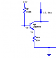
(See diagram)
In the diagram you can see from post #32 we ended the analysis with the circuit with Q1, and that part is shown there. We then concentrate on that section.
We know the input current is the current through RF:
iRF=(15-vb)/150000;
and the current through the emitter resistor is:
iRB2=iRF+0.0164;
thus the emitter voltage is:
ve=iRB2*220;
and it is also related to vb because of the diode drop:
ve=vb-0.7;
equating these last two we get:
iRB2*220=vb-0.7;
solving for vb we get:
vb=32475/7511
Back to the first equation:
iRF=(15-vb)/150000
replacing vb with the numerical value we get:
iRF=2673/37555000
and since this is the base current iB and we know iC=16.4ma=164/10000 we can calculate the Beta by dividing iC/iB:
Beta=(164/10000)/(2673/37555000)
and this gives us:
Beta=615902/2673
which with six digits is approximately equal to:
Beta=230.416
You should go over this and make sure everything is right.
Once we have this we can go on to look at some variations in both the Beta and small currents into the bases of the two driver transistor pairs and whatever else we'd like to know about. One thing we will find for example is that the circuit could really use the symmetrical output resistors usually found on these amplifiers as that helps to set the quiescent currents from those two driver pairs. There are other things to look at too through, such as the mismatch between the total voltage of the three diodes in series and the sum of the three base emitter voltages of the driver transistor pairs, which is what the symmetrical output resistors help to cure. The problem is if there is a difference in voltages the quiescent current in the drive transistors can end up going very high without these important resistors, especially when we are depending on diode voltage drops to match transistor base-emitter diode drops, which is not actually possible over all temperature values, and probably not even at room temperature.
The general idea here now is to go over the design using the calculations and see what would make the circuit more practical.
Attachments
-
 4.1 KB Views: 5