Industrial Universal IO circuit analysis found in the Industrial Controllers

Thread Starter

pralayp

Joined Apr 8, 2020
5
Hello All,
I'm new to this forum.
I have come across a universal IO controller from a reputed brand.
While studying the circuit, I came across the Universal Analog IO circuit(Supposedly) which can output 4-20mA and 0-10V from the same pin.
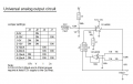
The circuit looks simple but I'm unable to analyze the working of it. Attached is the schematic.
Kindly help me understand the working and if the traced circuit is correct(However I have verified the same 2-3 times).

Thanks in Advance!!
 

Attachments

MisterBill2

Joined Jan 23, 2018
27,741
There is a whole lot about that circuit that does not look right to me.
FIRST, there is nothing similar to a current loop input circuit, which means it will not be able to accept any current loop input.
I suggest seeking a more capable source of circuits and abandon the source that provided that circuit.
 

Thread Starter

pralayp

Joined Apr 8, 2020
5
There is a whole lot about that circuit that does not look right to me.
FIRST, there is nothing similar to a current loop input circuit, which means it will not be able to accept any current loop input.
I suggest seeking a more capable source of circuits and abandon the source that provided that circuit.
Hello,
The circuit is traced from a working controller, so the functionality is unquestionable.
I can accept that there may be some mistakes from my team in the tracing activity.
If it were you designing the circuit, based on your experience what corrections would you make to make the circuit functional. Can you please provide a circuit for that. You may edit in the same schematic.
 

MisterBill2

Joined Jan 23, 2018
27,741
What is missing is the intended external circuit portion, providing an understanding of the intended operation of what we see.
Are we able to see the intended arrangement of the system for both the voltage and current output applications??
The problem on my end is not being able to see inside the thinking of other folks. And not being willing to make guesses.
 
Last edited:

MisterBill2

Joined Jan 23, 2018
27,741
C54 and D10 are shorted out
THAT was obvious. I took them to be options for some applications.
One confusion item is that it appears to have the input on the right-hand side and the output on the left side, opposite of the standard convention. UNLESS I have got it all backwards. THAT is a possibility that I can't ignore.
 

panic mode

Joined Oct 10, 2011
5,083
the original may be working but recreated schematics is something else. it certainly is buggy... and yes, it is drawn in a nonconventional way (both backwards and upside down), probably by someone trying to reverse-engineer what the original circuit is.

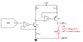
the DAC1 is node controlled by DAC. then U2A is used as an amplifier but... with an open loop gain. which makes no sense. then the amplified signal is used to drive the BJT buffer stage. this too is messed up. there is no reason for two transistors unless one of them is doing something else such as current limiter. the signal then goes through R55 to AOUT_P. R55 is used to sense output current - this is FEED2 signal. another opamp is used to do the same but on the low side of R55. of course this "low side" is not so obvious because of strange way circuit is drawn. SW1 allows selecting which feed to follow...
 

panic mode

Joined Oct 10, 2011
5,083
certainly there are current loops in serial comms but those are digital circuits while here TS specifically talks about industrial analog IO, for 0-10V and 4-20mA.
there are numerous designs of just such circuits with varying complexity...
https://www.ti.com/content/dam/vide...er_introduction_4-20ma_iout_0-10v_vout_fn.pdf
https://www.analog.com/media/en/reference-design-documentation/reference-designs/cn0229.pdf

or just use output for current but to turn it into a voltage output, introduce 500 Ohm resistor (via switch or additional terminal) like
1780220670436.png

or, DIY version with many options like:
1780220216645.png
 
Last edited:

MisterBill2

Joined Jan 23, 2018
27,741
The circuit presented in post #4 was "a building block portion" of some control scheme. And while the quality of building blocks is important, seeing one building block will seldom reveal the whole structure scheme or function. Certainly that is what I see in this case!!
Probably someone who is familiar with where that specific block fits into some control scheme to achieve some specific function in some useful manner.
What I can verify with certainty is: That person is not me!!
 

Fonhuaicho

Joined Apr 10, 2026
6
Universal I/O designs are always interesting because they have to handle different signal standards without sacrificing accuracy or protection. I'm particularly curious how the circuit switches between 0–10V and 4–20mA modes, and whether isolation is implemented at the input stage or elsewhere in the signal path. Looking forward to seeing the schematic and understanding the design trade-offs.
 

MisterBill2

Joined Jan 23, 2018
27,741
Universal I/O designs are always interesting because they have to handle different signal standards without sacrificing accuracy or protection. I'm particularly curious how the circuit switches between 0–10V and 4–20mA modes, and whether isolation is implemented at the input stage or elsewhere in the signal path. Looking forward to seeing the schematic and understanding the design trade-offs.
I am also wondering about how that is achieved!!
My observation for many years has been: "When one size fits all, it seldom fits any of them very well."
 
Top