CMOS analog delay cricuit

Thread Starter

penumbra

Joined Dec 8, 2012
76
BBD.png

Graph.png

Ron H,

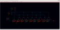
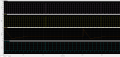
I have attached my simulation results and circuit.

The output doesn't seem to be quite like what i would want.

V1 and V2 are net 11 and net 7 respectively, showing the clocks for operating the gate of the NMOS.

V0 is the signal, basically it is a rough look like the action potential at the input.

Signal-out is the output.

All capacitors are 100femto F


Please help in analyzing.

Also, i downloaded the MN3207 data sheet from here which shows the simple circuit diagram:

http://www.datasheetarchive.com/MN3207-datasheet.html

What does Vdd and Vgg mean and where do they go


Thanks.
 
Last edited:

Thread Starter

penumbra

Joined Dec 8, 2012
76
have you had a look at these data sheets which have a fair bit of info design wise in them?

I have been looking at these, but i can't seem to get my design working in Cadence. Please look at my above attachments.

Can you help with what does Vdd and Vgg mean?
 

Ron H

Joined Apr 14, 2005
7,063
View attachment 51951

View attachment 51952

Ron H,

I have attached my simulation results and circuit.

The output doesn't seem to be quite like what i would want.

V1 and V2 are net 11 and net 7 respectively, showing the clocks for operating the gate of the NMOS.

V0 is the signal, basically it is a rough look like the action potential at the input.

Signal-out is the output.

All capacitors are 100femto F


Please help in analyzing.

Also, i downloaded the MN3207 data sheet from here which shows the simple circuit diagram:

http://www.datasheetarchive.com/MN3207-datasheet.html

What does Vdd and Vgg mean and where do they go


Thanks.
Your clocks appear to be identical. They need to be ≈180° out of phase. Look at the clock timing of the MN3207 VERY carefully. Note that they are non-overlapping.
According to the circuit on the last page of the datasheet, Vdd is 4 - 10V. The datasheet of MN3102 says Vgg=14/15*Vdd.
 

Thread Starter

penumbra

Joined Dec 8, 2012
76
Your clocks appear to be identical. They need to be ≈180° out of phase. Look at the clock timing of the MN3207 VERY carefully. Note that they are non-overlapping.
According to the circuit on the last page of the datasheet, Vdd is 4 - 10V. The datasheet of MN3102 says Vgg=14/15*Vdd.

Can i use an inverter to invert the clock of one relative to the other?
 

Thread Starter

penumbra

Joined Dec 8, 2012
76
Ron,

I've uploaded the new simulation results.

Please help me analyze the results.

There is clearly a delay at out_1, but what is happening at out_2?

Also, the voltage values of output signal have dropped a lot.

Clocks are running at 5v and 2000Hz and all capacitors are 100f F
All transistors are 0.35u length and 0.7u width.

I made this new BBD just like it shows in the MN3207 data sheet.


New_BBD_MN3207.png

new_run_graph.png
 

Ron H

Joined Apr 14, 2005
7,063
Its not clear to me what M9 and M10 do. I see them on the MN3207, but I don't understand how that part works. I don't understand what the devices connected to Vgg do.

Your output source followers should have pull-down devices of some sort - current sources or resistors or something. Otherwise, the only output you will get will be from gate-to-source capacitance.
 

Thread Starter

penumbra

Joined Dec 8, 2012
76
Its not clear to me what M9 and M10 do. I see them on the MN3207, but I don't understand how that part works. I don't understand what the devices connected to Vgg do.

Your output source followers should have pull-down devices of some sort - current sources or resistors or something. Otherwise, the only output you will get will be from gate-to-source capacitance.

Hi,

I tried the 2.3 Complementary output topology as shown in this website....

http://www.electrosmash.com/mn3007-bucket-brigade-devices


Please see if you can understand.
 

Ron H

Joined Apr 14, 2005
7,063
Hi,

I tried the 2.3 Complementary output topology as shown in this website....

http://www.electrosmash.com/mn3007-bucket-brigade-devices


Please see if you can understand.
Did you see this?
The output architecture was enhanced using two source follower transistors connected to the last two consecutive capacitors, resulting in a full wave output. Mixing these two outputs a more continuous output waveform is generated, providing a means of inproved suppression of clocking glitches. Some designs use a trimpot to vary the load termination between the two output followers to minimize clock frequency component due to VGS between them. This could be useful if running very low clock frequencies, and tight filter skirts to passband.
You have to have pulldown current sinks on each source follower, and resistive summing of those outputs, if I understand what they are saying.
 

Thread Starter

penumbra

Joined Dec 8, 2012
76
Did you see this? You have to have pulldown current sinks on each source follower, and resistive summing of those outputs, if I understand what they are saying.

So, on my attached circuit diagram, where do i add this pulldown current sink? Like should i tied the two outputs together?

Do i need to do this if i try the circuit 2.2 Tetrode Isolation Topology?

and what clock frequency should i use?
 
Last edited:

Thread Starter

penumbra

Joined Dec 8, 2012
76
Its not clear to me what M9 and M10 do. I see them on the MN3207, but I don't understand how that part works. I don't understand what the devices connected to Vgg do.

Your output source followers should have pull-down devices of some sort - current sources or resistors or something. Otherwise, the only output you will get will be from gate-to-source capacitance.

Ron H

Can you please try the 2.3 or 2.2 from the website electrosmash on your LT Spice and let me know? I would really appreciate your help!
 

Ron H

Joined Apr 14, 2005
7,063
So, on my attached circuit diagram, where do i add this pulldown current sink? Like should i tied the two outputs together?
The current sinks go from the source follower outputs to ground. You can use I elements to test different current levels, then implement them with transistors.


Do i need to do this if i try the circuit 2.2 Tetrode Isolation Topology?
I don't know. I like the source follower followed by a sample and hold, like I used in the circuit I posted.

and what clock frequency should i use?
A lower clock frequency gives you more delay per stage, but means you will need a more aggressive filter to get rid of the clock.

I'm going to bed.
 

Thread Starter

penumbra

Joined Dec 8, 2012
76
The current sinks go from the source follower outputs to ground. You can use I elements to test different current levels, then implement them with transistors.


I don't know. I like the source follower followed by a sample and hold, like I used in the circuit I posted.

A lower clock frequency gives you more delay per stage, but means you will need a more aggressive filter to get rid of the clock.

I'm going to bed.

Okay okay, thanks so far, just last question for now....
What is I element?

Also, why does your sample and hold have a v pulse?
 

Ron H

Joined Apr 14, 2005
7,063
Okay okay, thanks so far, just last question for now....
What is I element?
It's a behavioral current source. You should have one in Cadence. You know that V is a voltage source? Well, I is a current source. Turn it upside down, and it's a current sink.

Also, why does your sample and hold have a v pulse?
A sample and hold is a switch connecting a signal to a capacitor. Turn the switch on to sample the signal, charging it to the instantaneous signal voltage. Then turn it off to hold the sample on the capacitor. The V pulse is what turns the switch on.

Sample and hold.
 

Thread Starter

penumbra

Joined Dec 8, 2012
76
It's a behavioral current source. You should have one in Cadence. You know that V is a voltage source? Well, I is a current source. Turn it upside down, and it's a current sink.

A sample and hold is a switch connecting a signal to a capacitor. Turn the switch on to sample the signal, charging it to the instantaneous signal voltage. Then turn it off to hold the sample on the capacitor. The V pulse is what turns the switch on.

Sample and hold.
What type of filter should i implement? As you can see i have too many spikes in my output signal, even when the line is flat at the input. Any reasons for that?
 

Thread Starter

penumbra

Joined Dec 8, 2012
76
Ron,

Is it giving problems because of the negative component of the signal? I believe the NMOS won't respond well to the -ve voltage.
 

Ron H

Joined Apr 14, 2005
7,063
Hi,

If you look at the attached snapshots, the signal input is -ve for the latter half.

in any case, my signal has to concern the action potential, meaning if will have a -ve component
as shown here:

http://hyperphysics.phy-astr.gsu.edu/hbase/biology/actpot.html
You will have to level shift and amplify the action potential, as I did in my circuit. The optimum level has to be determined empirically. In my circuit, I amplified the action potential by 10 (E3 in the schematic), then level shifted it by 4V (V3 in the schematic).
Once you get the circuit simulation working, the best way to find the optimum level shift is probably by temporarily applying a sine wave, maybe at 10kHz, of various amplitudes and offsets, until you find a good combination that will yield the lowest harmonic distortion. Then you have to amplify and level shift your action potential until it has the same amplitude and DC level.

The reason for amplification is to minimize the signal-to-noise (or signal-to-clock) ratio at the output of your BB device.
Harmonic distortion is measured by looking at the FFT of the output. Cadence should have that capability. The input MUST be a sine wave when analyzing harmonic distortion.
 

Thread Starter

penumbra

Joined Dec 8, 2012
76
You will have to level shift and amplify the action potential, as I did in my circuit. The optimum level has to be determined empirically. In my circuit, I amplified the action potential by 10 (E3 in the schematic), then level shifted it by 4V (V3 in the schematic).
Once you get the circuit simulation working, the best way to find the optimum level shift is probably by temporarily applying a sine wave, maybe at 10kHz, of various amplitudes and offsets, until you find a good combination that will yield the lowest harmonic distortion. Then you have to amplify and level shift your action potential until it has the same amplitude and DC level.

The reason for amplification is to minimize the signal-to-noise (or signal-to-clock) ratio at the output of your BB device.
Harmonic distortion is measured by looking at the FFT of the output. Cadence should have that capability. The input MUST be a sine wave when analyzing harmonic distortion.
Thanks for the informative post. So what you mean is, that the entire waveform must be shifted vertically so that all of it appears only on the +ve side? and then that should be fed into the BBD?

How about i try to split the input signal into positive and negative part and then feed them separately? But how would that be implemented, like using the inverter?

Basically, right now i was thinking maybe my circuit is not giving the output as desired, as the input signal fluctuates b/w +ve and -ve.

If you see, you can clearly see some delay, however there are too many 'bars' or spikes in the output.
 
Top