Facebook
 Google
 GitHub
 Linkedin

Ron H,
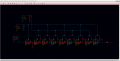
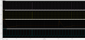
I have attached my simulation results and circuit.
The output doesn't seem to be quite like what i would want.
V1 and V2 are net 11 and net 7 respectively, showing the clocks for operating the gate of the NMOS.
V0 is the signal, basically it is a rough look like the action potential at the input.
Signal-out is the output.
All capacitors are 100femto F
Please help in analyzing.
Also, i downloaded the MN3207 data sheet from here which shows the simple circuit diagram:
http://www.datasheetarchive.com/MN3207-datasheet.html
What does Vdd and Vgg mean and where do they go
Thanks.
Last edited: