Facebook
 Google
 GitHub
 Linkedin


The below is an idea, I haven't try it yet, it might need some modification.
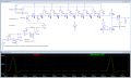
Signal → CD4066 In → Control pin → CD4066 Out → Signal delay for 1mS
Signal → Voltage comparator (> -7V) → negtive Voltage cut off circuit → 0.01uf → Ne555 mono 1mS Delay → NPN Transistor inverter → CD4066 control pin
The Power for CD4066 and Op Amp should be ≧ +7.5V,0,-7.5V.
Negtive Voltage cut off circuit, it will cut off the negtive voltage to protecting the NE555, the voltage only from 0 to +V.
The power of NE555 Only just need 0,+V.
Voltage comparator - ex: LM339,LM393 or Op amp As LM358, LM324.
CD4066 Control pin will actived by high.
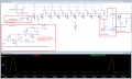
Signal → CD4066 In → Control pin → CD4066 Out → Signal delay for 1mS
Signal → Voltage comparator (> -7V) → negtive Voltage cut off circuit → 0.01uf → Ne555 mono 1mS Delay → NPN Transistor inverter → CD4066 control pin
The Power for CD4066 and Op Amp should be ≧ +7.5V,0,-7.5V.
Negtive Voltage cut off circuit, it will cut off the negtive voltage to protecting the NE555, the voltage only from 0 to +V.
The power of NE555 Only just need 0,+V.
Voltage comparator - ex: LM339,LM393 or Op amp As LM358, LM324.
CD4066 Control pin will actived by high.