3-Way Class D DSP Amp with Analog & Digital Inputs

Thread Starter

thepix

Joined Sep 11, 2026
4
Hey Guys,

In a quest of trying to build some 3-way studio monitors I've come up with the problem of powering them in the way I desire.

Simple route would be to spend money on 2 Hypex Amps and call it a day, but where's the fun in a DIY project that way...

So the goal is:
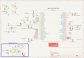
  • Single End and Balance input (Combo 3/4 Jack and XLR) and Toslink Digital I/O
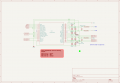
  • DSP for Filters, Room Correction, EQ Profiles
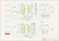
  • 3-Way Output 2x PBTL, 1x BTL
  • Post Filter Feedback circuit
  • Controllable LED indicator for current EQ Profile

I've been working solo on this for months on end, it's my first ever electronics project and now I'm not sure if I'm just doubting myself or most likely there are better ways to go about my current design so I'm here looking for some guidance.

Here's the current list of my concerns:
  • Controlling the input audio signal voltage and audio signal voltage at a number of stages on the way. There are maximums in the datasheets, but not sure whether or not I've mitigated for those along the way sufficiently?
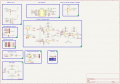
  • Power distribution, I have a +36V/+12V DC power supply to connect to the board, several component require +1V2, +1v8, +3V3, +5V, -12V and +12V. Have I used an efficient method for this and am I correctly supplying power from the various capacitors on the board?
  • Via Stitching, I probably should be using some, but should pointers would be great...
  • EEPROM/FastLED, wanted to be able to write data to EEPROM memory in slave mode to a ATTiny 404 as well as use it to control the LED with FastLED. Is this feasible, or would I need 2 separate ICs?
  • Fault/OC Protection/Reset circuits, are the current implications correct?
  • Just component choices, any better recommendations?
  • Also just recently dawned on me, with the Analog being converted to Digital before the output stage, how am I going to control volume levels?

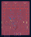
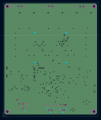
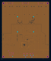
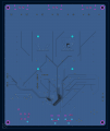
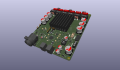
Attached the current schematics, I've also already mapped on a 4 layer board SGN&GND/GND/PWR/SGN&GND, so again any feedback on it all would be much appreciated.

I've also made the mistake of not planning ahead for the heatsink (who would've known it would be so hard to source specific sized ones), could've done with having the amps a little closer together to fit on the shelf heatsinks and I'm loathed to go back and move everything around...

Sorry for the long post!!
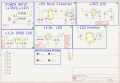
3-Way Class D Power Distribution.png3-Way Class D IO Board.png3-Way Class D DSP.png3-Way Class D DAC.png3-Way Class D Amps.png3-Way Class D PCB Front.png3-Way Class D PCB Ground.png3-Way Class D PCB Power.png3-Way Class D PCB Back.pngClass-D 3-Way Amp 3D.png
 
Hello, this is an interesting DIY project.
I've been comparing the blocks with the eval kit specs published by Analog Devices as well.
https://www.analog.com/media/en/tec...user-guides/eval-adau1452miniz_user_guide.pdf
and some components seem to be different.

I'm not sure how much audio fidelity will be affected by varying component choice and I've read from some other posts on similar DIY projects related to Hypex that there is always something wrong or something missed with other alternatives - unavailable parts, incompatible DSPs and connectors, cluttered cabling, unoptimized (poorly designed) amplifiers, lack of manufacturer support with some components as well as software updates etc. - factors I believe are polished by Hypex's R&D division.

All I can say from experience is to choose components with the highest bandwidth possible to minimize signal distortion.

Just out of curiosity, I'm wondering what the comment 'approved' means in the power input box (did it undergo testing)?

If you already used a fixed type for 1.2V and 1.8V, why not with the 3.3V LDO as well? (might be more accurate - though I don't think you need an exact 3.3V output with very low tolerance - and would save PCB space)

The BUCK converter is also bootstrapped, but might not be necessary (will save PCB space).

I only skimmed through uploaded materials, so please take all of my above ramblings with a grain of salt.

Hope the project becomes successful and competitive with Hypex's quality.

Cheers,
Justin
 

Thread Starter

thepix

Joined Sep 11, 2026
4
Just out of curiosity, I'm wondering what the comment 'approved' means in the power input box (did it undergo testing)?
Hi Justin,

Thanks for the reply. I had enlisted a bit of help to complete the PCB design, I think those are residual comments on his part at to where he was at. His PCB design was absolute garbage, so I used that schematic as the jump off point to start from fresh.


If you already used a fixed type for 1.2V and 1.8V, why not with the 3.3V LDO as well? (might be more accurate - though I don't think you need an exact 3.3V output with very low tolerance - and would save PCB space)
I thought all of the LDO's were the fixed variety rather than the variable ones?

I'll be happy if it works for a fraction of the Hypex cost:)
 

MisterBill2

Joined Jan 23, 2018
28,175
Certainly this is quite an ambitious project! I have not seen any obvious problems, although I have not done a circuit-schematic to PCB comparison for it. THAT check takes a lot of effort, I discovered long ago.

For the concern about "100MFD caps across the inputs, could it be that they should be 100 PICOFARAD capacitors? THAT value would be reasonable for RF bypass capacitors.

UNFORTUNATELY, this website schematic viewer does not allow a clear view of the whole circuit, so a careful evaluation would be rather difficult, at least for me.
So GOOD LUCK WITH THE BUILD!!
Please share with us when it is all completed and working!! It looks like it will be a usefull system!
 
Last edited:
I’d resolve the input-capacitor point that 0ri0n raised before going further with the PCB. If those really are 100 uF capacitors connected from the audio inputs to ground, their reactance is only about 1.6 ohm at 1 kHz, so they would heavily load the source. Check whether the intended connection was series AC coupling, or whether the value is incorrect.

Volume control can happen inside the DSP. The ADAU1452 evaluation-board guide actually demonstrates a clickless volume-control block on page 9. You can apply a common master volume to all three bands while retaining separate driver-level trims.

However, digital volume control cannot prevent the analogue input stage or ADC from clipping. I’d make a gain budget showing the maximum expected input, input-stage gain, ADC full-scale level, allowance for EQ boosts, DAC full-scale output and amplifier gain. Use the specified operating ranges and distortion performance, rather than absolute maximum ratings, as your design targets.

For the power supplies, start with a current estimate for every rail. LDO dissipation is approximately (Vin − Vout) × I: dropping 12 V to 3.3 V at 100 mA already produces 0.87 W. Also, whether an LDO is fixed or adjustable depends on its complete part number; the schematic symbol alone won’t establish that.

For the PCB layout, I’d prioritise a continuous ground plane, short decoupling loops and separation between the switching outputs and low-level analogue inputs. This article on Class-D amplifier layout illustrates those points, including ground connections and thermal vias. It uses an older STA517B design, so follow your particular amplifier’s datasheet for component values, exposed-pad connections and thermal requirements.

Post-filter feedback deserves a separate validation step. The output filter and speaker impedance become part of the feedback loop, so component substitutions need a stability check. TI’s PFFB application report is useful background, although its component values apply to the listed TPA324x/325x implementations.

I’d bring up the supplies first, then the DSP/converters, then one amplifier channel into a suitable dummy load. Keep the amplifiers muted until the DSP and clocks are ready. Resolve the heatsink mounting before ordering boards, too.

Could you upload readable PDF schematics? That would make checking the actual connections and part suffixes much easier.
 

Thread Starter

thepix

Joined Sep 11, 2026
4
Analog inputs (balanced + single ended) are shorted to ground by 100uF caps.
Now that you've mentioned it and looking back, I'm not even sure how they got there. Might be residual from that shyster off Freelancer I had work on a PCB design for me...

Good looking out, thanks!!
 

Thread Starter

thepix

Joined Sep 11, 2026
4
@lichurbagan Firstly, thanks for the detailed reply, very much appreciated let's go one by one.

I’d resolve the input-capacitor point that 0ri0n raised before going further with the PCB. If those really are 100 uF capacitors connected from the audio inputs to ground, their reactance is only about 1.6 ohm at 1 kHz, so they would heavily load the source. Check whether the intended connection was series AC coupling, or whether the value is incorrect.
As per previous reply, this has now been addressed. I've looked over what I was trying to replicate (c&f) and the datasheet and the caps are nowhere to be seen, so must of been from the previous design.

Volume control can happen inside the DSP. The ADAU1452 evaluation-board guide actually demonstrates a clickless volume-control block on page 9. You can apply a common master volume to all three bands while retaining separate driver-level trims.

However, digital volume control cannot prevent the analogue input stage or ADC from clipping. I’d make a gain budget showing the maximum expected input, input-stage gain, ADC full-scale level, allowance for EQ boosts, DAC full-scale output and amplifier gain. Use the specified operating ranges and distortion performance, rather than absolute maximum ratings, as your design targets.
Yes, I'd prefer it not to be buttons so I'll probably have to have some potentiometer and connect it to an ADC#. I have a couple on 2.54mm connectors on the board, so I guess that can work. Guess it was just one of those lightbulb moments and now the latter is going to be something new for me to research, but glad now I know...

For the power supplies, start with a current estimate for every rail. LDO dissipation is approximately (Vin − Vout) × I: dropping 12 V to 3.3 V at 100 mA already produces 0.87 W. Also, whether an LDO is fixed or adjustable depends on its complete part number; the schematic symbol alone won’t establish that.
I had watched some videos on this topic, which my understanding was going from higher voltage say 12V down to a 1.2V creates a lot more heat and energy to deal with, which is why I went down in stages with LDO's from 5V > 3.3V, 3.3V > 1.8V and 1.8V> 1.2V. I did specifically choose the fixed LDO's, the part numbers are on the schematic denoted by the last 2 digits e.g. TLV76733DRV and TLV76718DRV so should be good there.

For the PCB layout, I’d prioritise a continuous ground plane, short decoupling loops and separation between the switching outputs and low-level analogue inputs. This article on Class-D amplifier layout illustrates those points, including ground connections and thermal vias. It uses an older STA517B design, so follow your particular amplifier’s datasheet for component values, exposed-pad connections and thermal requirements.
I'll defo take a read of the Class-D amplifier layout article, had a quick scan seems similar to the TPA3251EVM design which I took my cues from, but this is a write up rather than mainly images... The continuous ground plane and short decoupling loops @m sure have been taken into consideration. You'll have to remind me what my switching outputs are relative to my analog inputs though.

Post-filter feedback deserves a separate validation step. The output filter and speaker impedance become part of the feedback loop, so component substitutions need a stability check. TI’s PFFB application report is useful background, although its component values apply to the listed TPA324x/325x implementations.
This is what I followed and I'm using the TPA3251's so this should be good to go...

With all that said, I've also attached the pdf version of the schematics.
 

Attachments

Top