How to make a clocked CMOS Inverter in Cadence virtuoso.

WBahn

Joined Mar 31, 2012
32,786
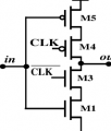
I have done this way in cadence but Iam not getting a proper output. Is the below reference circuit diagram correct?
What do you consider a "proper" output?

Have you actually looked at your circuit for each of the four possible input conditions to see what you expect the output to be for that circuit (regardless of what you might want the output to be)?

Your attachment text claims that this is a latch of some kind. On what is that claim based?
 

Thread Starter

Makers

Joined Dec 29, 2024
8
What is a clocked inverter?
A clocked Cmos inverter is a inverter which includes pmos and a nmos but it is controlled by a clock when the clock signal is high the output changes as a normal inverter do but when clock signal is low it holds the previous output.
 

MrChips

Joined Oct 2, 2009
34,758
A clocked Cmos inverter is a inverter which includes pmos and a nmos but it is controlled by a clock when the clock signal is high the output changes as a normal inverter do but when clock signal is low it holds the previous output.
By that description, I would call it a data latch with inverting output.

Note the difference between a D-type flip-flop and a data latch.
With a D-type flip-flop, the output changes only on the proper edge of the clock.
With a data latch, the data flows through (inverted in your case) while the clock is HIGH.

Draw the schematic of a data latch first using logic gate symbols. After that, you can design the circuit with CMOS transistors.
 

Thread Starter

Makers

Joined Dec 29, 2024
8
What do you consider a "proper" output?

Have you actually looked at your circuit for each of the four possible input conditions to see what you expect the output to be for that circuit (regardless of what you might want the output to be)?

Your attachment text claims that this is a latch of some kind. On what is that claim based?
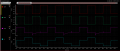
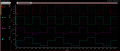
Yes, I have looked at my circuit. The outputs are floating, they are not giving output as high and low. I have attached the screenshot below:
 

Attachments

Thread Starter

Makers

Joined Dec 29, 2024
8
By that description, I would call it a data latch with inverting output.

Note the difference between a D-type flip-flop and a data latch.
With a D-type flip-flop, the output changes only on the proper edge of the clock.
With a data latch, the data flows through (inverted in your case) while the clock is HIGH.

Draw the schematic of a data latch first using logic gate symbols. After that, you can design the circuit with CMOS transistors.
Here is the screenshot which I have done using cmos transistors. The problem is that the outputs are floating. They are not giving proper high and low.
 

Attachments

Top