Three stages power amplifier school project

Thread Starter

Lucky-Luka

Joined Mar 28, 2019
181
Hi all
I do have a school project to do: a 3 stages power amplifier circuit.

+-16V power supply
+- 175mV input signal swing corresponding to +- 14V output swing. (closed loop voltage gain = 80).
open loop gain of the 3 stages ampli = 2450
resistive load >= 10ohm
amplifier input resistence >= 10kohm
bandwidth >=80 kHz
phase margin 80°
efficiency >=60%
THD <=1%

I have to use only transistors listed in the ltspice database.
That's why I had to choose 2N3055 (npn) and D45H11 (pnp): the only ones capable of dealing with 10W power dissipation (I've read that from their datasheets).

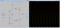
I've started the project from the output stage.
Class AB output stage using a Vbe multiplier as biasing and a current mirror (current source as first attempt).
I just wanted to see if I could get it right... Something went wrong... Obviously...
I gave it a 14V sinusoidal input with -1.3 DC offset and I hoped to see sinusoidal 14V oscillating around 0V as vo.
I got a distorted sinusoidal waveform oscillating around -280 mV.
How can I fix that? What am I doing wrong?
Any suggestions is appreciated.
Cheers
 

Attachments

Last edited:

Audioguru again

Joined Oct 21, 2019
6,674
Your circuit is missing the DC and AC negative feedback that all amplifiers have. The DC negative feedback will fix the DC offset and the AC negative feedback will fix distortion.
Why do you think that each output transistor must dissipate 10W? The output voltage swing is 14V peak which is 9.9V RMS. Then the output power is 9.9V squared/10 ohms= 9.8W. The efficiency is supposed to be 60% so the total dissipation shared by both output transistors is 6.6W. Then each output transistor dissipates 6.6W/2= 3.3W. With a good heatsink, a 2N3055 can dissipate 80W and its max output current is 15A. The peak output current in your amplifier is only 14V/10 ohms= 1.4A so why use such powerful output transistors?

EDIT: Of course the output transistors need emitter resistors since each transistor is different.
 

Thread Starter

Lucky-Luka

Joined Mar 28, 2019
181
Why do you think that each output transistor must dissipate 10W? The output voltage swing is 14V peak which is 9.9V RMS. Then the output power is 9.9V squared/10 ohms= 9.8W. The efficiency is supposed to be 60% so the total dissipation shared by both output transistors is 6.6W. Then each output transistor dissipates 6.6W/2= 3.3W. With a good heatsink, a 2N3055 can dissipate 80W and its max output current is 15A. The peak output current in your amplifier is only 14V/10 ohms= 1.4A so why use such powerful output transistors?
Where does 6.6W comes from?
BTW is this the way to compute the total dissipation? I think I've seen several projects where it was computed the way I did (which led me to 9.8W).

EDIT: Of course the output transistors need emitter resistors since each transistor is different.
Why do I need them?
Which values should be ok and why?

I have improved the output stage.
A big question arises now: how is it possible that I get almost 50W as avarage power across power transistor Q1?!
Thanks
 

Attachments

AlbertHall

Joined Jun 4, 2014
12,345
This is supposed to be class AB, no?
With no input signal there should be only a very small current through the output transistors but that circuit gives a current around 3.2A.
The voltage across Q5 is too great. That voltage is particularly critical as you have no emitter resistors for Q1 and Q3.
 

Thread Starter

Lucky-Luka

Joined Mar 28, 2019
181
This is supposed to be class AB, no?
With no input signal there should be only a very small current through the output transistors but that circuit gives a current around 3.2A.
The voltage across Q5 is too great. That voltage is particularly critical as you have no emitter resistors for Q1 and Q3.
How can I improve my circuit? Just emitter resistors? What are they for? Which values?
Thanks
 

AlbertHall

Joined Jun 4, 2014
12,345
No. The resistors give some stability to the quiescent current.
The magnitude of that current is set by the voltage across Q5.
The offset of the input voltage sets the quiesecent output voltage to zero.
This latter should be set by feedback from the output to the driver transistor - but you haven't got one of those.
R8 is that feedback resistor in the circuit below:
1576794618309.png
 

Audioguru again

Joined Oct 21, 2019
6,674
Transistors are not all made the same. Some will have a Vbe of 0.6V, others 0.7V and many will be in between. An emitter resistor adds to the Vbe and therefore reduces the effect of the voltage differences.
 

ronsimpson

Joined Oct 7, 2019
2,989
How did u choose the appropriate voltage?
I played with Q5 B-C resistor and the output transistor Emitter resistors.
The red trace in for one transistor and the green trace is current in the other transistor. Blue is output voltage.
Note at zero voltage out the current in each transistor is 100mA. This could be set with the input signal=0V.
I used chose 1.6 watts in each transistor when nothing is happening. (lost power but needed)
Both transistors need to be a little bit on at 0V or there will be cross over distortion. (bump in the signal at 0V)
1576802500396.png
 

Audioguru again

Joined Oct 21, 2019
6,674
Your 7.2W amplifier shows low distortion. Its output transistors are powerful enough to produce 25W into a 2 ohm speaker.
I noticed that Parts Express has replacement 1 ohm speakers for a (9 speakers) Bose 901 speaker system. Each speaker is 4.5" and is rated for 30W RMS.
 
Top