 Facebook
 Google
 GitHub
 Linkedin
Hi everyone,
I’m facing issues with my nRF52 BLE design due to a solder mask thickness change and grounding approach. I’d appreciate expert guidance on retuning the Pi filter, recalculating impedance, and resolving grounding concerns.
Issues Faced:
- Solder Mask Thickness Change:
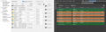
- Ref NRF52 DK design: Solder mask thickness = 0.0175 mm.
- My design: Solder mask thickness = 0.035mm. See image 1.
- Impact: Impedance mismatch and high resistance readings (~MΩ) at the decoupling capacitor near the antenna and radio ground pin.
- Grounding Concern:
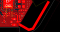
- Recommended Approach: Radio ground pin should connect to the decoupling capacitor via a trace before connecting to the ground plane. See image 2.
- Current Design: The radio ground pin connects directly to the ground plane using vias, bypassing the decoupling capacitor.
- Impedance Mismatch:
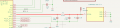
- Pi filter components (C1=0.8 pF, L=3.9 nH, C2=0.5 pF, C3=1.2 pF) were designed for the previous solder mask thickness. See image 3.
- With the updated solder mask, the effective dielectric constant and parasitic values have changed, resulting in potential impedance mismatch at 2.4 GHz (BLE frequency).
- How to recalculate C1,C2,C3,C_1, C_2, C_3,C1,C2,C3, & LLL for 50 Ω matching? Tools/methods?
- How to adjust for 0.035 mm solder mask thickness and recalculate microstrip impedance?
- Should the radio ground pin route through the decoupling capacitor instead of direct via to the ground plane?
- Best way to validate updated design (e.g., S11, VNA settings)?
- Design Context:
- PCB: FR4 material.
- Frequency: 2.4 GHz (BLE).
- Antenna: Custom trace antenna.
- Tools Available:
- Saturn PCB Toolkit, AppCAD, and access to a VNA for measurements.
- Objective: Achieve optimal impedance matching and address potential grounding-related performance issues.
Attachments
-
 121 KB Views: 3
 -
 227.6 KB Views: 4
 -
 46.9 KB Views: 4


