 Facebook
 Google
 GitHub
 Linkedin
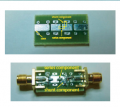
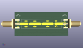
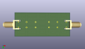
My goal is to create a prototyping board that I could use for two types of passive, LC ladder filters using 0603 components. Attached you will find images of the objective and 3D views of the PCB's front and back. Before I send the Gerber files to the facility for manufacturing, it would greatly help me if someone with experience in these processes could review these and help me answer these questions:
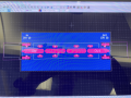
1. Should the vias underneath the SMA pads remain there or be moved from their locations?
2. Why do I get DRC error messages stating that I have vias either unconnected or connected to only one layer when I either move the vias underneath the pads from under the pads or add stitching vias?
3. Can you identify changes that would improve the functioning of my board?
The design is a 2-layer PCB using FR4 with a total thickness of approximately 1.6 mm. The copper layers are each 0.035 mm, and there is a bottom, ground plane.
Thanks for your help.
Attachments
-
 101.6 KB Views: 9
 -
 164.6 KB Views: 9
 -
 128.7 KB Views: 9
 -
 3.4 MB Views: 7


