Facebook
 Google
 GitHub
 Linkedin
Hi all, I’m new to PCB design and working on my first board. I’ve breadboarded everything and now want to make a PCB that holds the core modules and lets me expand later.
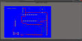
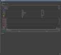
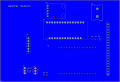
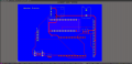
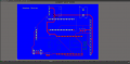
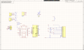
Components: – ESP32 Dev Module V1 – Arduino Nano – 2× DS18B20 – BME280 – BH1750
Current issues:
1. The ESP32 footprint was imported from Eagle and the outlines are spread across mechanical layers.
All feedback is welcome — I’m trying to learn and improve.
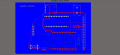
Components: – ESP32 Dev Module V1 – Arduino Nano – 2× DS18B20 – BME280 – BH1750
Current issues:
1. The ESP32 footprint was imported from Eagle and the outlines are spread across mechanical layers.
- 2. I plan to mount the ESP32 and Nano using headers so I can swap them out.
All feedback is welcome — I’m trying to learn and improve.
Attachments
-
 203.8 KB Views: 5
 -
 65.4 KB Views: 6
 -
 140.4 KB Views: 6
 -
 196.6 KB Views: 5
 -
 193.2 KB Views: 4
 -
 210.9 KB Views: 4
 -
 133.4 KB Views: 4