Design Review Request - ESP32-P4 Control Board

Thread Starter

Dirus

Joined Jan 9, 2016
22
Hello Everyone!

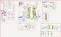
I'm new to the world of Electronics design and have a Control system I've been designing based around a Waveshare ESP32-P4 Module.

High level overview is a smart controller that can monitor the status of a door, operate a solenoid, view USB cameras, connection and control done via Wifi/Ethernet with tie-in to various Home Automation systems, and voice assistants.

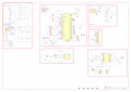
Power is either from a external 48v power supply or via 802.3bt Poe++ with the optional "Ethernet Module", 5v, 3.3v, & 12v (solenoid voltage) are on converted on seperate "Power Supply cards". (Done this way for ease of repair reasons)

There is an onboard RJ45 jack that is meant for connecting "Daughter Boards" that can be daisy chained. These basically contain their own buck conversion, USB Hub, Solenoid & Sensor circuits etc.

So far I've spent about the past month pouring over Datasheets, and Evaluation Design Documents, and picking apart various circuit designs to get to this point.

That said, I've come as far as I can with the limited knowledge I have and I'm hoping to get some guidance on what I'm missing, what can be changed etc.
 

Attachments

Irving

Joined Jan 30, 2016
5,068
I was going to say 'Welcome to AAC' but you've been a member longer than me!

Is this a rehash of an existing board, hence the big red Xs on connectors etc.?

General observations:

Sub-circuits, eg solenoid circuit, should be drawn with signal flow left->right, power at top, ground at bottom (else the electrons get confused ;) )

You have a good smattering of 100nF decoupling capacitors, but you need more bulk capacitance 1 - 10u spread around, though exactly where depends on layout to some extent.

Layout of this is going to be quite daunting. Certainly not a beginners project without some guidance, but we can cross that bridge when we get there!

How do you plan to program/debug this board?

Some obvious issues:

Pin1 of reset switch needs to go to the R3/C2 junction, not to 3.3v

You have a short between Q1 drain and+12v

Position sensor input - not sure what the sensor is, but why the zener? Needs some series resistance before C1 to provide filtering.

You need a pull-down resistor (10k) from Q1 gate to ground.

C18/C19 on SCL/SDA, why? Generally need to minimise capacitance here.
Scrap the variable resistors on SCL/SDA. Use higher values here then have additional resistors on daughter boards to 'parallel up' as needed. plus you already have 4k7 on each at USB Hub.

Resistor values for 12v monitor (to give approx 2.5v as per 48v, 5v and 3.3v) - R41 should be 39k. Though 2.5v is on the high side, normal ADC input on ESP32 is 1.1v unless you program the internal attenuator. It would be better to aim for 1v, giving resistor values of R40/R42/R44/R46 =1k, R39=47k, R41=11k, R43=4.02k (or 3k9 + 100), R45=2.32k (or 2k2 + 100) - depends how accurate/critical you want to be. TBH, unless the 3.3v rail is good you aren't going to be worried about the other rails.

What's with the weird combo of resistors on the power rail LEDs? The actual resistance isn't that critical. assuming 2v LED @ 2mA, standard values are: 48v 22k, 12v 10k, 5v 1k5, 3.3v 680

Are TVS1 and TVS2 meant to be back to back (48v rail)? There's little value in having 2 of them.


I'm sure there are other things to check, but that'll keep you busy for a bit :D
 
Last edited:

MisterBill2

Joined Jan 23, 2018
27,323
Please consider, if you want others to be able to follow the function and flow, that a collection of small segments gives no hint as to what the system actually does.
I AM AWARE that this style of presentation is used by some folks and probably works well with automated PCB layout software.
BUT for us mere humans, IT IS VERY HARD TO FOLLOW THE SIGNAL FLOW with isolated blocks that have a four-character identifier for every connection to other blocks.
IN FACT, I would not accept such a design drawing from any designer.

Consider the future use of a system schematic drawing document:
Three main uses: First, for the design evaluation, where the design is evaluated against the list of requirements,
second, for the construction of an actual physical copy of the circuit to be the core of a system, often a machine of some variety,
and finally, for some individual who is tasked with servicing the machine that has ceased to operate in the manner that it is intended to operate, and which it has ceased to operate in that same manner.
The signal or data flow must be visible, and hopefully, obvious, for the evaluation and the service functions. That requires a visible connection that conveys the flow paths, and that mostly requires a graphic presentation that connects the functions in the correct sequence.
 

Thread Starter

Dirus

Joined Jan 9, 2016
22
I was going to say 'Welcome to AAC' but you've been a member longer than me!
I joined years ago when I was trying to fix a color shift issues on a TV, ended up fixing it by heatsinking the part that was going out. I haven't been back since as back then I wasn't really interested in anything that wasn't more mechanical.

I'm a old Mechanic turned Fire Alarm Technician these days and alot more into the more electrical/electronic side of the world now.

Is this a rehash of an existing board, hence the big red Xs on connectors etc.?
It's a completely custom board, the Red X's signify that the parts are marked "do not populate", essentially a way to get 2.54mm pitch through holes arranged so that either a header can be soldered in that place, or wires can be inserted and soldered.

General observations:
Sub-circuits, eg solenoid circuit, should be drawn with signal flow left->right, power at top, ground at bottom (else the electrons get confused ;) )
And here I thought I did a decent job with the flow and layout of the schematic, I'll see about cleaning it up a bit more later on. :)

You have a good smattering of 100nF decoupling capacitors, but you need more bulk capacitance 1 - 10u spread around, though exactly where depends on layout to some extent.
Yes, I would agree there, placement is heavily layout dependant, I just don't have enough knownledge as to how many and where.

Layout of this is going to be quite daunting. Certainly not a beginners project without some guidance, but we can cross that bridge when we get there!
Would you believe I more or less have all the PCB layouts done as the schematic sits at this point?, it even passes DRC with the JLCPCB 4 layer constraints.

Main PCB.png


Main PCB 3D.png


How do you plan to program/debug this board?
Programming via USB, and I have a Phone App in the works to communicate over either Bluetooth or Wifi.

Some obvious issues:
Pin 1 of reset switch needs to go to the R3/C2 junction, not to 3.3v
Fixed.

You have a short between Q1 drain and+12v, You need a pull-down resistor (10k) from Q1 gate to ground.
Fixed? Looks like I had that circuit wired all wrong,

Drain is now attached to the Solenoid Negative.

Gate connected to GPIO41 with a 1k in series,

Source is connected to GND.

The SS34 is now strapped across the solenoid positive and negative rails.

Position sensor input - not sure what the sensor is, but why the zener? Needs some series resistance before C1 to provide filtering.
The sensor type can vary, in most instances though it will be a simple NO switch. The zener provides protection to the GPIO pin in 2 ways, by clamping voltage spikes either from latent voltage in the wiring or parasitic inductance to ground , and in conjunction with the debounce capacitor protects against mechanical bounce effects.

Most likely the wiring for the solenoid and the position sensor will be run together.

C18/C19 on SCL/SDA, why? Generally need to minimise capacitance here.
Scrap the variable resistors on SCL/SDA. Use higher values here then have additional resistors on daughter boards to 'parallel up' as needed. plus you already have 4k7 on each at USB Hub.
By C18/C19, I assume you mean C15/C16 on the I2C bus, these are essentially low pass filters since the circuit can run through 1 or more Cat6 cables between cards picking up noise, so they help shunt that noise to ground.

The number of daughter cards can range from 0-4, you have variable lengths of Cat6 runs between the daughter cards, each daughter card has 2 I2C devices, and the number of I2C devices on both this controller and the daughter boards is expandable. I figured that the variable resistors are more or less the easiest way to tweak the performance of the I2C bus given how many unknowns there are when deploying the system.

Resistor values for 12v monitor (to give approx 2.5v as per 48v, 5v and 3.3v) - R41 should be 39k. Though 2.5v is on the high side, normal ADC input on ESP32 is 1.1v unless you program the internal attenuator. It would be better to aim for 1v, giving resistor values of R40/R42/R44/R46 =1k, R39=47k, R41=11k, R43=4.02k (or 3k9 + 100), R45=2.32k (or 2k2 + 100) - depends how accurate/critical you want to be. TBH, unless the 3.3v rail is good you aren't going to be worried about the other rails.
12V rail is kind of a misnomer, the rail is fed by an MP9486 and is adjustable by changing the values of it's R1/R2 on the power supply board, in this case R2 is actually a 10k potentiometer allowing upto a maximum of 36V. Some use cases may require 12v, others 24v or 36v. That's why those resistor values are present.

What's with the weird combo of resistors on the power rail LEDs? The actual resistance isn't that critical. assuming 2v LED @ 2mA, standard values are: 48v 22k, 12v 10k, 5v 1k5, 3.3v 680
The LED indicators were a late addition to the design. The resistors were originally picked as I was trying to keep the number of unique part #'s on the BoM as low as possible for when I get the boards produced and those values already existed, for example I do not have a 22k in use anywhere else but I do have 10k and 1k resistors already on the board, thus by using them I'm cutting production costs.

Are TVS1 and TVS2 meant to be back to back (48v rail)? There's little value in having 2 of them.


I'm sure there are other things to check, but that'll keep you busy for a bit :D
From what I was able to find using 2 in parallel provides a better protection circuit, it slightly lowers the overall clamping voltage and increases reaction time, TVS1 primarily handles fast ESD/EFT events coming from the cable or external PSU, while TVS2 provides secondary protection against slower surges or residual noise that propagates through the first stage.


Thank you for all your help so far!
 

Thread Starter

Dirus

Joined Jan 9, 2016
22
Please consider, if you want others to be able to follow the function and flow, that a collection of small segments gives no hint as to what the system actually does.
I AM AWARE that this style of presentation is used by some folks and probably works well with automated PCB layout software.
BUT for us mere humans, IT IS VERY HARD TO FOLLOW THE SIGNAL FLOW with isolated blocks that have a four-character identifier for every connection to other blocks.
IN FACT, I would not accept such a design drawing from any designer.

Consider the future use of a system schematic drawing document:
Three main uses: First, for the design evaluation, where the design is evaluated against the list of requirements,
second, for the construction of an actual physical copy of the circuit to be the core of a system, often a machine of some variety,
and finally, for some individual who is tasked with servicing the machine that has ceased to operate in the manner that it is intended to operate, and which it has ceased to operate in that same manner.
The signal or data flow must be visible, and hopefully, obvious, for the evaluation and the service functions. That requires a visible connection that conveys the flow paths, and that mostly requires a graphic presentation that connects the functions in the correct sequence.
This is the first schematic I've ever created, I've spent about a month teaching myself electronics, design, and how to use KiCad.


This style of design I picked up from the ESP32/KiCad community. The vast majority of schematics I've gone through have been layed out more or like this.

Waveshare which is who manufactures this ESP32-P4-32MB Module publishes the schematics of all their boards in a similar style, tho I find theirs to be even less intuitive, but that could just be I'm new to a lot of the terms used.

I tried to lay out everything in sections, Power related on the left, main ESP32-P4 module related in the center, and end user interfaces and outputs on the right.

Each section is squared off with a Header explaining what that section is, and extra explanations such as why I used a potentiometer over a fixed resistor in a certain section value for example.

Power related labels are always pointed up, ground is always pointed down, GPIO pins etc are left and right and labeled to explain what it's doing instead of just the pin name (48VDC_MON for example goes to the ADC Pin responsible for monitoring the voltage on the 48VDC rail). The labels are arrowed, pointing to something it's an input, pointing away it's an output, pointed on both sides is bi-directional.

Drawing wires from every point to every point instead of labels I feel would look way too chaotic.

Repairability wise down the line is where documentation comes into play, every industry has their own way of doing things. Automotive wiring diagrams are vastly different from electronics diagrams, which are vastly different from PLC Ladder Logic diagrams, which are vastly different from Fire Alarm blueprints that contain 2 completely different styles on the same print(Floorplan and Single Line).

I'm curious if you even looked past the style at the actual schematic?, or if you just saw something akin to four character identified blocks and decided you couldn't be bothered and instead decided to issue a lecture on why it's wrong in your opinion to do it this way and how you'd never hire someone like me who designs this way.

Whether or not you'd be willing to hire me based on my first ever schematic because of a style I picked up that you admit some people use is irrelevant to me. This is a hobby project for me.
 

Irving

Joined Jan 30, 2016
5,068
This is the first schematic I've ever created, I've spent about a month teaching myself electronics, design, and how to use KiCad.
Kudos!

I have no issue with this style of schematic as I use it myself. Dave Jones of EEVBlog fame has a great video on the subject of good practice in drawing schematics

I would recommend this video on PCB layout as well (and many others in his blog)
 

Thread Starter

Dirus

Joined Jan 9, 2016
22
Kudos!

I have no issue with this style of schematic as I use it myself. Dave Jones of EEVBlog fame has a great video on the subject of good practice in drawing schematics

I would recommend this video on PCB layout as well (and many others in his blog)
Thank you!

I'll have to check out both of those videos and do some rearranging on the schematic layout.

I'll post up the newest version of the schematic later today.
 

MisterBill2

Joined Jan 23, 2018
27,323
In a 40 year engineering career I have created and delivered a few hundred circuit drawings that were used to build and service assorted equipment and machines. AND while circuits of individual modules were part of that list, those were modules that also had to be built. In addition, I did usually include detailed drawings of cable assemblies that included detailed connector pin-outs and cable lengths.

" I'm curious if you even looked past the style at the actual schematic?, or if you just saw something akin to four character identified blocks and decided you couldn't be bothered and instead decided to issue a lecture on why it's wrong in your opinion to do it this way and how you'd never hire someone like me who designs this way. "

Really, I looked very carefully at the posted drawing!
And I saw that It was obviously organized and not "a random stack" of snippets.
My response was not at all a jump to be critical!!

The fact that some "user communities" follow a particular style does not mean that it is what works best for those folks in the industry who actually build machines and systems, or those who need to service the systems a year later.

AND, I have not presnted that sort of drawing to a customer's design review group for project approval, either. Those presentations were always subject to pointed criticizems for whatever was not considered adequate.
As a "detailed Block Drawing" it would be quite good, actually, with the arrangement matching the actual connections.
 

ericgibbs

Joined Jan 29, 2010
21,419
Hi,
The TS has asked for guidance on his circuit design, not a critique of his drawing method.

Please keep to topic.

Moderation.
 

Thread Starter

Dirus

Joined Jan 9, 2016
22
Made the corrections suggested by Irvine. The reset switch, and the incorrectly hooked up MOSFET driving the Solenoid circuit.

Overall, I flipped a bunch of sections so they travel left to right and up to down, added more header info, renamed all the remaining labels that had just "GPIOXX" to their actual function. Highlighted the various sections of the main ESP32 with a pointer to what seperate area they're fed to.
 

Attachments

Irving

Joined Jan 30, 2016
5,068
Are you sure you posted the corrected files, as I don't see much change around the solenoid circuit...

Here are some correctly drawn examples of solenoid output and ESP Reset snippets.. makes it so much easier to understand what's going on... 'current' always flows left to right and top to bottom...

1775558618089.png
 

Thread Starter

Dirus

Joined Jan 9, 2016
22
Only difference between my solenoid circuit now and yours is I don't have R2. I'll add it.

My old circuit had the SS34 connected to the +12v, and both it and the connector for Solenoid - went directly to ground.

I rotated it on the schematic as I had the connector on the left, I just forgot to flip it over so that positive is up and ground is down.

Same with the Reset Switch, I need to flip it, Pwr up Gnd down.
 
Top