 Facebook
 Google
 GitHub
 Linkedin
Hello everyone,
Following the feedback I received in my previous thread(mentioned below), I’ve completed a full redesign of the board and would appreciate another review before moving forward with fabrication. The goal of this revision was not incremental fixes, but addressing the underlying issues identified earlier and reworking the design accordingly.
This is the most complex PCB I’ve designed so far. While I’ve worked previously on smaller boards (breakouts, sensor modules, power boards), this design integrates high-speed interfaces, mixed-signal circuitry, and mechanical constraints, so I want to be cautious before committing to production.
Previous thread (for context):
https://forum.allaboutcircuits.com/threads/first-time-pcb-design-review.208961/
Summary of changes since the previous revision
All major points raised in the earlier discussion have been implemented and verified in this redesign.
Key updates include:
Design overview
What I’m specifically looking for feedback on
I’ve attached schematics and key PCB layers below. Any feedback—whether small layout improvements or major architectural concerns—would be greatly appreciated before I move to fabrication.
Thank you for your time and expertise.
----------------------------------------------------------------------------------------------------------------------------------------------------------
What I’m most worried about in this revision:
If any areas appear marginal rather than outright incorrect, I’d especially appreciate comments on those as well.
===============================================================================================
Note: At first glance, it may appear that all the THT pin headers have a courtyard error—however, this is not the case. While a two-row THT pin header could have been used, it would make the schematic more difficult to interpret. The pin headers are intentionally arranged so that each is spaced 2.54mm apart from the others, resulting in a pitch of 2.54mm.
P.S. Attaching PDF files based on comments from the previous post. I will post KiCAD files on your request.
Following the feedback I received in my previous thread(mentioned below), I’ve completed a full redesign of the board and would appreciate another review before moving forward with fabrication. The goal of this revision was not incremental fixes, but addressing the underlying issues identified earlier and reworking the design accordingly.
This is the most complex PCB I’ve designed so far. While I’ve worked previously on smaller boards (breakouts, sensor modules, power boards), this design integrates high-speed interfaces, mixed-signal circuitry, and mechanical constraints, so I want to be cautious before committing to production.
Previous thread (for context):
https://forum.allaboutcircuits.com/threads/first-time-pcb-design-review.208961/
Summary of changes since the previous revision
All major points raised in the earlier discussion have been implemented and verified in this redesign.
Key updates include:
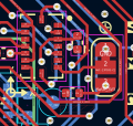
- USB connector redesign:
The USB connector has been changed from a THT part to an SMD variant to address the mechanical and signal-integrity concerns noted previously. This required reworking the USB routing and connector placement. - Addition of components
A buzzer has been added to the circuit.
- Complete mechanical restructuring:
The board has been redesigned to follow common COTS(Commercial-Off-The-Shelf) flight-controller form factors, using 30.5 mm × 30.5 mm mounting holes.
Component placement has been completely reworked based on routing efficiency, mechanical clearance, and functional grouping. - Improved protection and signal integrity:
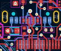
- Series resistors added on selected timer outputs to limit MCU pin current.
- Series resistors were added on selected high-speed clock signals to improve edge quality(avoid ringing).
- Power routing and local decoupling were reviewed and updated.
- USB differential pair redesign:
- Differential impedance calculated explicitly(similar to the previous one, with JLCPCB values as reference).
- Controlled routing applied.
- Measured length skew ≈ 1.5 mm
- General cleanup based on prior feedback:
- Improved grounding strategy.
- Cleaner routing based on NetClass rules(screenshot attached).
- Better separation of noisy and sensitive circuitry(separating the timer channel from the main 5V).
- Added stitching vias at certain places.
- Updated a few footprints.
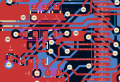
Design overview
- MCU: STM32H743
- Input voltage: 5 V (from a previously designed external power board)
- VBAT: Used only for voltage monitoring via MCU ADC
- EDA tool: KiCad 8.0.7
- Mechanical format: 30.5 mm × 30.5 mm mounting pattern
What I’m specifically looking for feedback on
- Power routing, decoupling strategy, and return paths
- USB connector choice, placement, and ESD robustness
- Component placement and mechanical practicality
- Manufacturability and assembly risks
- And any obvious “this will fail on first power-up” issues
I’ve attached schematics and key PCB layers below. Any feedback—whether small layout improvements or major architectural concerns—would be greatly appreciated before I move to fabrication.
Thank you for your time and expertise.
----------------------------------------------------------------------------------------------------------------------------------------------------------
What I’m most worried about in this revision:
- USB signal integrity around the SMD connector and ESD placement
- High-speed return paths for SPI and SD card signals across plane transitions
- Power integrity and noise coupling into the IMU and MCU analog domains
- Whether any layout decisions look acceptable on screen, but risky in practice
- Subtle manufacturability issues that may not be obvious during design
- Silkscreen advice to make it look more professional
If any areas appear marginal rather than outright incorrect, I’d especially appreciate comments on those as well.
===============================================================================================
Note: At first glance, it may appear that all the THT pin headers have a courtyard error—however, this is not the case. While a two-row THT pin header could have been used, it would make the schematic more difficult to interpret. The pin headers are intentionally arranged so that each is spaced 2.54mm apart from the others, resulting in a pitch of 2.54mm.
P.S. Attaching PDF files based on comments from the previous post. I will post KiCAD files on your request.
Attachments
-
620.5 KB Views: 2
-
271.3 KB Views: 1
-
 217.5 KB Views: 4
 -
 201.9 KB Views: 4
 -
 224.9 KB Views: 3
 -
 15.2 KB Views: 3


