The label at each component on a schematic is called a Reference Designator. In a proper schematic, *each and every* component has a unique one. Without them, discussing the functions or diagnosing problems are cumbersome - saying something is the upper right resistor just doesn't cut it on a schematic with 100 parts.
Here are some standard prefixes:
B - battery
C - capacitor
D - diode
J - jack
K - relay
L - inductor
P = plug
Q - transistor
R - resistor
SW - switch
T - transformer
U - integrated circuit
V - vacuum tube
X - various
Y - crystal
Vcc - Voltage, common collector, generally the positive operating voltage for the circuit. Technically, only for bipolar parts. Since this design uses CMOS parts, it should be Vdd (Voltage, drain). You use this symbol when you don't know what the voltage will be. For these parts it can be anything from 3 V to 18 V, but for the circuit it is the relay operating voltage, 5 V or 12 V.
A very common practice is not to show power and ground connections to ICs. This came out of digital logic schematics in the 60's, where all TTL parts had +5 V and GND connections in the opposite corners. Removing all of the criss-crossing power wires made the schematics much more clear. Because opamps do not have the uniformity that logic parts have, many people show opamp power connections. BTW, C2 and C3 (see how unambiguous that was?) are power supply decoupling capacitors, one for each IC (U3 is a transistor array and doesn't need one). These should be placed as close as possible to each device's power and ground (Vdd and Vss) pins.
Parts with multiple sections, such as a hex inverter or quad opamp, use modifiers. The four opamps in an LM324 would be U1A, U1B, U1C, and U1D. Search for something like 'power supply schematic' or 'function generator circuit' and you will get hundreds of examples under images. Once you get past the overload, you will see patterns and common features, like ground symbols always point down, positive voltage sources are up and negative ones are down, inputs to the left and outputs to the right, etc. These are not hard and fast rules, but conventions that have coalesced over time.
Way before the internet (or even arpanet), I spent all of sophomore English class sitting in the back of the room reading a mentor's entire collection of Popular Electronics. A good schematic is crafted like a story. There is a structure and flow to the information. The primary function of a schematic is to show the *electrical* (not physical) relationships among the components. It often works out that the way the parts are arranged on the page is similar to the way they wind up on a pc board, but forcing the physical arrangement into the schematic usually makes the schematic harder to read. Notice on my schematic that the pin numbers are not in sequence for all parts. They are arranged to make the signal patterns easier to see. This is partly because the ICs do not have the signals pinned in sequential order, but mostly because a schematic with a zillion crossed lines is self-defeating (and painful). In my design library I have seven (7) different symbols for the CD4060, with various locations for the Reset and oscillator pins, different output patterns, etc.; all to make the schematic easier to read. The layout is determined by the physical part characteristics, and is out of your control. No reason to make your life more difficult by pulling that mess into the schematic.
Hi AK
I have nearly built the circuit by am cautious abt the power supply to U1 and U2. Need to check this with you before I energise it and possibly blow it up.
I assume all ICs have to have their own connection to a power supply.
I note that the data sheets for U1 and U2 specify the power pins as "VSS = 8" and "VDD = 16". You have left them off yr circuit diagram. Is there any reason for this? I am inferring from your post above that it's just convention to simplify the graphic.
As a corollary, it's my understanding that earth/ ground equates to the negative supply line. So for example pin 12 of U1 and pin 13 of U2 as per your schematic (earthed) will become common with pin 8 on U1 and pin 8 on U2. Is this correct?
Also, U3 pin 9 labelled by you as VCC will become common with pin 16 of U1 and pin16 of U2 (VDD/ +ve/ V+/ VS+).
A common "feature" of most schematic drafting (design entry) programs is the ability to hide nets, yet maintain their connectivity through attributes of the component symbols. In the 60's, large schematics started happening, full of logic gates. Since all of the parts ran on 5 V and GND, those pins were left off of the drawings to reduce clutter. So in my design library, the component decal has the power and ground pins defined with an associated net name, such as pin 8 = GND. The schematic ground symbol has one pin with the same attribute, and the program invisibly connects the two. This matters because the program outputs a "netlist", a text file that defines every component and connection. PC board layout programs import the netlist, and it is there that all physical connections are visible. All of this is a massive inconvenience for a beginner, having to remember which categories of connections might be missing from a schematic.
CMOS confuses things because the name for the positive power pin is Vdd, not Vcc. So sometimes on a schematic you will see a Vcc and Vdd symbol connected together but not to any other parts. This is a way to tell the netlist generator how to manage the invisible power pins with different net names.
Vcc = Vdd = power source positive output.
GND - Vss = power source return (negative output)
In your case there is no true negative power source, such as +12 V. This would be called Vee by us geezers, and just -12 by everyone else.
Hello AK
I built the circuit but it's not working.
I have checked over the wiring several several times.
Clutching at straws, but I need to ask: should your circuit have positive power at junction of R3, C1 and R2?
My power supply is 6VDC.
Pin 10 of ULN2003 stays stuck on 4.8VDC. Will not advance. There is about 1V on the other six output pins. Placement of shunt at P1 makes no difference eve
Did you connect the power and ground pins that are not shown in the original circuit? I like to show the power connections on my circuits, but a lot of packages do not.
CD4060B and 4017B pin 8 to gnd, pin 16 to +6V
Maybe add an LED to pin 5 of the 4060, LED cathode to the pin, anode to 1K resistor and other end of the resistor to 6V.
Blinkinlights are a must
Then you can see if it is running.
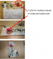
Dendad I connected an LED to pin 5 of CD4060 as u suggested. It's blinking and responsive to the pot R1. I had already connected the power rails to the 2 ICs as u suggested thx to an earlier post from AK. Is there another diagnostic test you can suggest? Perhaps there is something I can do to test function of IC 4017B. Or maybe there is a way to temporarily strip down and simplify the IC 4017B circuit so as to isolate it's operation.
Put a resistor from pin 15 to ground.
A 1k should work, but so will a 10k.
The 4017 circuit has no defined state for the reset pin so it probably is floating to reset the chip.
And if you want to see if it works without waiting for the 5 mins, connect pin 14 of the 4017 to maybe pin 6 instead of pin 3 and it will cycle quicker,
Once you get it going, I'll show you a way to get variable times for each relat, and have them overlap if you like.
I think I had some bad connections on the bread board. There was nothing wrong with @AnalogKid 's circuit!! And there was nothing wrong with my build of it either! I was despondent until you got me to put the blinking LED in. That told me that at least the first stage was wired correctly and gave me a much needed invencentive to keep looking for faults. After pushing everything down it suddenly started to work.
Your suggestion to connect the pin 14 to pin 6 and not pin 3 is great for testing. Now I know how to make it cycle quickly I have got much more immediate feedback if I tweek something.
Now it's working I can read up on the ICs and understand exactly what they are doing.
(Each time I get a project to work and before I move on to the next project I would like to write a story explaining to myself exactly how the circuit works and paste it into my exercise book.)
The jumper lead works to limit the number of outputs of the relay driver as per @AnalogKid 's design.
I have done everything you said and I can get it to cycle very quickly. (And v slowly) it's amazing.
A common "feature" of most schematic drafting (design entry) programs is the ability to hide nets, yet maintain their connectivity through attributes of the component symbols. In the 60's, large schematics started happening, full of logic gates. Since all of the parts ran on 5 V and GND, those pins were left off of the drawings to reduce clutter. So in my design library, the component decal has the power and ground pins defined with an associated net name, such as pin 8 = GND. The schematic ground symbol has one pin with the same attribute, and the program invisibly connects the two. This matters because the program outputs a "netlist", a text file that defines every component and connection. PC board layout programs import the netlist, and it is there that all physical connections are visible. All of this is a massive inconvenience for a beginner, having to remember which categories of connections might be missing from a schematic.
CMOS confuses things because the name for the positive power pin is Vdd, not Vcc. So sometimes on a schematic you will see a Vcc and Vdd symbol connected together but not to any other parts. This is a way to tell the netlist generator how to manage the invisible power pins with different net names.
Vcc = Vdd = power source positive output.
GND - Vss = power source return (negative output)
In your case there is no true negative power source, such as +12 V. This would be called Vee by us geezers, and just -12 by everyone else.
 Facebook
 Google
 GitHub
 Linkedin
")