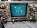
Push buttons on Trio CS-2070 Oscilloscope are not responding and some constantly engaged

MrAl

Joined Jun 17, 2014
13,859
Ok. I'll try all this. It might take me some time. I also tend to think it must be something digital for example to do with one of the many IC's. I have no idea how I would find out which one(s) though. I looked for some sort of error code based on the active led lights but I couldnt find anything


Hi mate. This scope is advertised at 70Mhz
Hello again,

Oh that's not bad at all. I would have killed to have a 70MHz scope 40 years ago, but even today that's not bad really.
Today the ratings are not up to par though. You get a 100MHz scope it may be only 30MHz.

It may be hard to fix this scope they are fairly complicated inside. I had one a long time ago that had arcing coming out of the input probe, I had to change the HV transformer because it had some kind of leakage. I ruined a very good calculator with it before I got around to fixing it.

If you can locate a trace that is in the group and that whole group is bad, you might see where that leads to.
To figure out if it is the switches themselves, see if they are single pole single throw. If they are, you can simulate pressing one by shorting out the contact pins with a jumper or even just a screwdriver or knife or something. If that works, you know for sure it's the switch.

You do not always have to replace a switch with the very same kind as long as you are willing to retrofit a different one or ones in place of the old. I had to do that with lots of stuff in the past because I could not get the exact part for replacement. That included capacitors that were bigger than the originals. If there are a lot of switches that need to be replaced, consider building a whole new switch panel with the new switches. If I could have replaced some of the membrane switches I had problems with in the past with regular switches, I sure would have.
 

Thread Starter

Tp86

Joined Sep 13, 2023
216
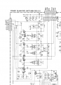
On the Vertical Attenuator PCB, all the connections marked in red should be at 5v and go to 0v when the relevant button is pressed. The orange ones should be 5v, the green 0v, the pale blue some voltage >= 5v (I think) and the brown approx 2.5v (or a squarish wave if you have another 'scope, or if this is working sufficiently). If all that's correct we can move on to the next level...

View attachment 345762
Hi. Updating what I've done:

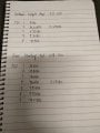
- I tried what you and nsaspook suggested regarding the vertical attenuation board and I can confirm all switches are functioning ok - voltage to gnd is high when not pressed and low when pressed. The high voltage is more around the 4vdc mark though so I don't know if that would cause an issue? Irving those pale blue and brown voltages are all 4.36vdc. It seems a bit different to what you expected?
 

Attachments

Thread Starter

Tp86

Joined Sep 13, 2023
216
If you can locate a trace that is in the group and that whole group is bad, you might see where that leads to.
To figure out if it is the switches themselves, see if they are single pole single throw. If they are, you can simulate pressing one by shorting out the contact pins with a jumper or even just a screwdriver or knife or something. If that works, you know for sure it's the switch.

You do not always have to replace a switch with the very same kind as long as you are willing to retrofit a different one or ones in place of the old. I had to do that with lots of stuff in the past because I could not get the exact part for replacement. That included capacitors that were bigger than the originals. If there are a lot of switches that need to be replaced, consider building a whole new switch panel with the new switches. If I could have replaced some of the membrane switches I had problems with in the past with regular switches, I sure would have.
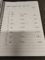
Thanks for those tips. I was able to verify the switches at least for the mode selections are with volt meter. What would you try next? Test diodes and resisters on the board the switches plug into?
 
Last edited:

nsaspook

Joined Aug 27, 2009
16,503
Hi. Updating what I've done:

- I tried what you and nsaspook suggested regarding the vertical attenuation board and I can confirm all switches are functioning ok - voltage to gnd is high when not pressed and low when pressed. The high voltage is more around the 4vdc mark though so I don't know if that would cause an issue? Irving those pale blue and brown voltages are all 4.36vdc. It seems a bit different to what you expected?
The pull-up voltages are OK on the switches but I don't really like the logic bus supply voltages.
You can try this.

Be really careful and check all the power supply connector pin voltages here. The +5.0V and +5.2V reads low on those other boards. They would push the normal TTL +5V supply to +5.2V at the regulator to compensate for wiring and board voltage drops so there would be close to +5V at the chip pins because they didn't use PS voltage sense lines to correct for voltage drops. You need to check the P22 voltage between GND pin 3 and +5.2 pin 5 on the power blanking board. This +5.2V output needs to be correct for proper operation of the digital circuits. The +7V regulator input supply on P20 pin 5 also needs to be correct. Need the DC volts and the AC volts (to check for ripple) on that +5.2 and +7V carefully with the rest of the regulator in/regulator out voltages. Bad/old caps might be causing high ripple on those critical for digital DC lines.
https://www.powerelectronicsnews.com/power-supply-design-notes-how-to-measure-ripple/

1743471579967.png
 
Last edited:

MrChips

Joined Oct 2, 2009
35,280
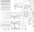
Study the circuit diagrams shown in posts #19 and #20.

You will see that CH2 INV goes to IC2d pin-9.
IC10a Q output is on pin-1, /Q output is on pin-2. These two outputs are complementary and should change state every time the button is pressed.

Similarly, ADD goes to IC1c pin-5 which leads to IC3b pin-6. You should see some level changes at the gates there.

Trio Kenwood CS-2070 switches.jpg
 

Thread Starter

Tp86

Joined Sep 13, 2023
216
The pull-up voltages are OK on the switches but I don't really like the logic bus supply voltages.
You can try this.

Be really careful and check all the power supply connector pin voltages here. The +5.0V and +5.2V reads low on those other boards. They would push the normal TTL +5V supply to +5.2V at the regulator to compensate for wiring and board voltage drops so there would be close to +5V at the chip pins because they didn't use PS voltage sense lines to correct for voltage drops. You need to check the P22 voltage between GND pin 3 and +5.2 pin 5 on the power blanking board. This +5.2V output needs to be correct for proper operation of the digital circuits. The +7V regulator input supply on P20 pin 5 also needs to be correct. Need the DC volts and the AC volts (to check for ripple) on that +5.2 and +7V carefully with the rest of the regulator in/regulator out voltages. Bad/old caps might be causing high ripple on those critical for digital DC lines.
https://www.powerelectronicsnews.com/power-supply-design-notes-how-to-measure-ripple/

View attachment 345804
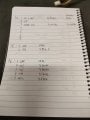
I have some results below:
- That p20 you said above is actually p30 (hard to read) so I went and measured wrong plug but ived remeasured p30 and pin 3 is 6.97vdc and no detected AC voltage on my meter
- p22 has a lower than expected voltage of 4.95vdc
- p22 which I posted earlier in thread also has 4.95vdc

Do you think the lack of 5.2V could be the issue?
 

Attachments

nsaspook

Joined Aug 27, 2009
16,503
I have some results below:
- That p20 you said above is actually p30 (hard to read) so I went and measured wrong plug but ived remeasured p30 and pin 3 is 6.97vdc and no detected AC voltage on my meter
- p22 has a lower than expected voltage of 4.95vdc
- p22 which I posted earlier in thread also has 4.95vdc

Do you think the lack of 5.2V could be the issue?
The 5.2v regulator is lower than the spec but it's close to 5.0 with little ripple so that voltage is likely not the root issue. I was hoping it was something simple but it seems not.
 

Thread Starter

Tp86

Joined Sep 13, 2023
216
The 5.2v regulator is lower than the spec but it's close to 5.0 with little ripple so that voltage is likely not the root issue. I was hoping it was something simple but it seems not.
I tested the scope on trigger mode and the trigger mode seems to work at least (I only tested CH1) None of the trigger mode bush buttons light up however but at least is triggering

Thank you for all the help so far on this. I guess there's not much else we can try
 

Attachments

Irving

Joined Jan 30, 2016
5,195
Oh there's lots more, we've hardly started!

The logic chips are all MC14000 series CMOS spec'd for 3 - 18v VDD, so 4.95v on 5v rail is of no consequence, IMHO.

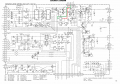
More concerning, to me, is the fact that the CONT and /CONT signals are both at 4.96v.... when you look at the source of these they come from the input and output of an inverter, IC8a, on the Horizontal Mode Control board, see highlighted schematic below, so should be complementary, shouldn't they?

It seems to me that +5.2VL and +VM are both driven via diodes (D20, D31) from +5VS via L1. As far as I can make out this is some sort of power interlock, requiring the 2 x 5v rails to be present at the collector of Q4, to change the state at the emitter, which is CONT and then the output of IC8a is /CONT.

CONT appears to be instrumental in enabling clock pulses to several flip-flops, while /CONT when low enables the outputs of several drivers. Could this be the source of the problem?

Screenshot 2025-04-01 111946.png
 

Thread Starter

Tp86

Joined Sep 13, 2023
216
Study the circuit diagrams shown in posts #19 and #20.

You will see that CH2 INV goes to IC2d pin-9.
IC10a Q output is on pin-1, /Q output is on pin-2. These two outputs are complementary and should change state every time the button is pressed.

Similarly, ADD goes to IC1c pin-5 which leads to IC3b pin-6. You should see some level changes at the gates there.

View attachment 345805
I think I see what you mean here. So on your CH2 INV example the IC10a is acting as a flip plop. Each time the switch is pressed the Q and Q-bar should switch states. I can definitely check this.

On the diagram I didnt see a similar Q and Q-bar output for the IC1c example you posted. The diagram only says Pin 5 in Pin 6 out
1743504750160.png
 

Thread Starter

Tp86

Joined Sep 13, 2023
216
Oh there's lots more, we've hardly started!

The logic chips are all MC14000 series CMOS spec'd for 3 - 18v VDD, so 4.95v on 5v rail is of no consequence, IMHO.

More concerning, to me, is the fact that the CONT and /CONT signals are both at 4.96v.... when you look at the source of these they come from the input and output of an inverter, IC8a, on the Horizontal Mode Control board, see highlighted schematic below, so should be complementary, shouldn't they?

It seems to me that +5.2VL and +VM are both driven via diodes (D20, D31) from +5VS via L1. As far as I can make out this is some sort of power interlock, requiring the 2 x 5v rails to be present at the collector of Q4, to change the state at the emitter, which is CONT and then the output of IC8a is /CONT.

CONT appears to be instrumental in enabling clock pulses to several flip-flops, while /CONT when low enables the outputs of several drivers. Could this be the source of the problem?

View attachment 345821
Wow. That is an impressive analysis. I need a bit more time to go over some of this as its a bit beyond me. I'm still learning to real some of these circuit symbols. Let me have a sleep and I'll get back to you:)
 

MrAl

Joined Jun 17, 2014
13,859
Thanks for those tips. I was able to verify the switches at least for the mode selections are with volt meter. What would you try next? Test diodes and resisters on the board the switches plug into?
Hi,

How did you verify the switches were all working properly themselves?

I am wondering if there is something programmable in the circuit. If there is, it is possible that the programming went bad due to some memory type going bad.
It's very hard to tell without having the unit right here in front of me, and even then it could be very hard to understand the exact problem.

Just have to ask a question here. Why do you buy stuff that does not work, is it because you want to gain experience fixing these products? That would be a good reason BTW. I just hope you did not pay too much for this scope.
 

MrChips

Joined Oct 2, 2009
35,280
I tested the scope on trigger mode and the trigger mode seems to work at least (I only tested CH1) None of the trigger mode bush buttons light up however but at least is triggering

Thank you for all the help so far on this. I guess there's not much else we can try
As Irving has stated, we have only just started. At this level of diagnostics, we don't test individual components. We check for functional behaviour of circuits.

The standard procedure is to check all operational voltages. Once they have been verified, in your case, I am 99% certain that this is a logic problem. Since the components are standard discrete logic ICs, there is a good chance that we can pinpoint the problem.

Once you have the VERTICAL ATTENUATOR UNIT board in a safe position where the ICs can be tested while fully powered, we can proceed.

CAUTION: It is imperative that you do not create accidental shorts while probing at the circuits. This will only make matters worse.

In order to examine pulsed outputs, you will need a working oscilloscope. Without that, we will have to make do with static measurements using a DMM set to measure voltage.

STEP #1
The first step is to check the supply voltages at the logic ICs. Vcc is 5 V. Thus, 4.95 V is perfectly acceptable.

STEP #2
We have two paths to check, the ADD signal and the CH2 INV signal. Let us focus on the CH2 INV signal alone for now. It is very likely that there is one common fault that is inhibiting both functions.

Follow the signal path of CH2 INV.
At IC2d pin-9, the voltage should be +5 V (nominal) and goes to 0 V when the CH2 INV button is pressed.
For safety, it is better to test the voltage at R92.

Next, the signal at IC2d pin-8 and IC7d pin-13 should be the opposite, i.e. the voltage should be +5 V when the button is pressed.

IC7 is an AND gate. If the voltage at IC7 pin-8 and pin-12 is not at +5 V, the signal will not propagate through the AND gate.
I will put my money on this being the case.

To be continued after you have checked the above.
 

Irving

Joined Jan 30, 2016
5,195
I am wondering if there is something programmable in the circuit. If there is, it is possible that the programming went bad due to some memory type going bad.
It's very hard to tell without having the unit right here in front of me, and even then it could be very hard to understand the exact problem.
There's nothing programmable here as far as I can see, its all old-school CMOS & TTL logic and a bunch of discrete transistors for power management...
 

nsaspook

Joined Aug 27, 2009
16,503
I tested the scope on trigger mode and the trigger mode seems to work at least (I only tested CH1) None of the trigger mode bush buttons light up however but at least is triggering

Thank you for all the help so far on this. I guess there's not much else we can try
There's a lot more to try but at least now it's useful as a scope.

The low 5.2V (the extra 0.2 volts is usually a part of the reliability/temperature range of operation design requirements) could be an indicator of trouble elsewhere. Did you measure that voltage unloaded (with the connector removed) or was it connected an powering the other boards. If the disconnected connector voltage reads 5.2V on that pin then the 5.2V bus might be loaded down due to a high current fault(s) somewhere else. I've used voltage drops like that to narrow down higher than normal fault conditions by disconnecting boards one by one.
 

Irving

Joined Jan 30, 2016
5,195
STEP #2
We have two paths to check, the ADD signal and the CH2 INV signal. Let us focus on the CH2 INV signal alone for now. It is very likely that there is one common fault that is inhibiting both functions.
I think the problem is broader than this and on the other PCB, however this will be a good and straightforward test of that and will give the OP some confidence in testing at the logic level. My guess is that this will all check out OK, and because CONT is high at IC7d pin 12, IC10a will happily toggle. BUT, because /CONT is also high (which it shouldn't be) the buffer, IC11d, on IC10a Q output blocks further transmission of this signal (and all like it) to the actual memory circuit on the other board. It turns out, as described in the manual a the top of page 2-3 that all the switch states are encoded and stored in registers on the Horizontal Mode Control Board and this state is maintained across power cycles so the 'scope always powers up in the state it was when powered down. The power rail +VM is Volts Memory and is maintained by a 1000uF capacitor. A good chunk of this CMOS logic is powered up even when the 'scope is off, hence all the tristate buffers. CONT high , /CONT low is the normal operating state and the reverse is the powered off memory state, except its locked somewhere between the two because both signals are high for some reason. If we find that, I see no reason why it won't spring back to life.
 

MrChips

Joined Oct 2, 2009
35,280
@Irving Obviously, you have looked more deeply into this than I have. I have not examined the design and consequences of having the oscilloscope's states stored during power down. Thanks for revealing this.
 
Top