PCB Production EasyEDA

Thread Starter

salhi

Joined Nov 29, 2023
86
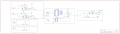
I have this circuit schematic that i made in easyeda, i want to make the PCB Layout of it but only over the copper layer, and keep the components on the top components layer, but then i faced many problems , i want to make all the traces with the width of 1.2mm, beside the energy supply inputs that will have 3mm in width, i failed to do the routing automatically so i went down the manual route, but im stuck i cant do anything to make it with my routing, any help is appreciated; here is the schematic file, along with a picture if anyone could make it routable, i would be grateful, thanks
 

Attachments

samunal

Joined Jul 3, 2024
26
If you want to do autoroute just go to autoroute setting and set the design rules. Add the trace and set it to the required width. here is an image you can follow: BTW, from where will you order the PCBs.
Screenshot_2024_08_07-1.pngScreenshot_2024_08_07-1.png
 

Thread Starter

salhi

Joined Nov 29, 2023
86
If you want to do autoroute just go to autoroute setting and set the design rules. Add the trace and set it to the required width. here is an image you can follow: BTW, from where will you order the PCBs.
View attachment 328688View attachment 328688
Hey sam, i tried this, but it fails many paths arent routed, it only succeed when doing routing on both components and copper side simultaneously
 

Jon Chandler

Joined Jun 12, 2008
1,560
There's no reason not to have tracks on top and bottom. The board cost will be the same for a single or 2 layer board.

In general, autorouters suck and most people don't use them. Treat board layout as a game, trying to find the most efficient layout. Rotating or moving components may may routing much easier.
 
Top