Non-inverting NFet gate driver

kubeek

Joined Sep 20, 2005
5,796
As for board space, you're right about that. But wouldn't this circuit be more reliable and last longer than the IR2101?
IR2101 is a 600V chip, which will have a big impact on die size and therefore price. There are single low side drivers available that will be cheaper, just because two 2A fets and a bit of logic don´t take as much chip space as when you add a 600V isolation distance. As for reliablility, I doubt there will be any difference, and the chip will likely be better characterized than your disrete circuit regarding reliablility and absolute limits.

For reliability calculations, our safety engineers need to know the number of transistors in said IC, and the reliability of ICs is more or less logarithmic to the number of transistors used, whereas reliability of discrete transistors is linear. So for a hundred thousand transistors in an Ic you would get reliability of say 1000 FIT (failures in 1e9 hours), but for hundred thousand discrete transistors it would be more like 20,000 FIT.
...but I'm under the impression that the 2n3904 and/or 2n3906 are less susceptible to ESD or spurious surges in voltage than a driver ic.
ICs have internal protecion diodes, discrete circuits generaly don't. Even though cmos structures are susceptible to shoothrough, that is exactly why the protection diodes are a rather large part of the die and why those might actually make them less susceptible to ESD and other EMC damage or degradation, than your discrete circuit might be.

Sorry for making it sound so complicated. In other words, it is easier to ensure that the input of an IC doesn't exceed 20mA no matter what, than to analzyze a discrete circuit and take into account all the factors that might bring you over the edge.
 

Thread Starter

cmartinez

Joined Jan 17, 2007
8,856
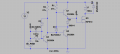
please delete teh top 5V source and connect R4 directly to the 12V rail
Just did, and it worked beautifully, thanks.
Call me conservative, but to me that is quite a lot of wasted power.
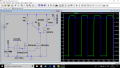
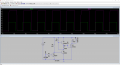
Hey, I consider it a compliment when somebody calls me conservative :) ... Anyway, I adjusted the values of R1 and R2 to 27k, and it barely made a dent in the circuit's performance. The top part of the rising edges of the gate signal rounded a little bit, but that's all.
upload_2018-4-20_18-48-49.png​

Then there's the question of frequency. An ic driver might easily outperform my last circuit, but I intend to work this circuit to a maximum of 40KHz ... in this case, there seems to be a delay of a little over 2 us between the falling edge of the driving signal and the gate... is there a way to minimize this without complicating things too much?
 

Attachments

RichardO

Joined May 4, 2013
2,270
... in this case, there seems to be a delay of a little over 2 us between the falling edge of the driving signal and the gate... is there a way to minimize this without complicating things too much?
The simplest way is to change the transistors Q2 and Q3 to 2n2369's (PN2369). Note the 15 volts maximum spec, though.

Putting Baker clamps on Q2 and Q3 will help some but not as much as changing the 2N3904's to 2N2369's.

upload_2018-4-20_19-56-33.png
 

Attachments

Thread Starter

cmartinez

Joined Jan 17, 2007
8,856
The simplest way is to change the transistors Q2 and Q3 to 2n2369's (PN2369). Note the 15 volts maximum spec, though.

Putting Baker clamps on Q2 and Q3 will help some but not as much as changing the 2N3904's to 2N2369's.

View attachment 150970
upload_2018-4-21_11-18-12.png
​
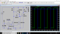
Thanks Richard, those clamps definitely improved performance. Now falling edge delay is only 0.2µs instead of 2µs, that's a 10x improvement! ... Anyway, it bothered me that the gate's voltage never went down to zero on the low part of the waveform, so I placed a 2k2 pull down transistor to ground, and now it fully reaches 0V after approx 2µs. I don't know if that's important, because without it the gate's lowest point is about 0.8V. According to the NFet's datasheet the minimum threshold voltage at the gate is 2V, so we should be ok. But I'd rather have the driver consume a little more power just to be on the safe side.
 

Attachments

Thread Starter

cmartinez

Joined Jan 17, 2007
8,856
I am sorry
The short-term and numerous breakdown of the Base Emitter transition leads to degradation of the transistor gain.View attachment 150996
That's a very interesting chip, the 74ahc1g14. I looked it up, and its datasheet says that "They provide an inverting buffer function with Schmitt-trigger action. These devices can transform slowly changing input signals into sharply defined, jitter-free output signals."
I don't have any with me for this project, but I'll definitely keep it in mind for future applications. Many thanks for your help.
 

Jony130

Joined Feb 17, 2009
5,600
.. Anyway, it bothered me that the gate's voltage never went down to zero on the low part of the waveform,
Without this 2k2 pull-down resistor, the voltage at the MOSFET gate is "set" by the Q2 Vbe2 and Schottky diode D4 forward voltage and D1 diode voltage.

Vgs_low = (Vbe2 - Vf4) + Vf1

Vgs_low_max = Vce2_(sat) + Vf1 ≈ (Vbe2 - Vf4) + Vf1 ≈ 0.7 - 0.3V +0.7 = 1.1V

Vgs_low_min = Vce2_(sat) ≈ (Vbe2 - Vf4)≈ 0.7 - 0.3V ≈ 0.4V at DC
 

Thread Starter

cmartinez

Joined Jan 17, 2007
8,856
I found this circuit while searching for something else, and the capacitive switching of the gates drew my attention.

AC MOSFET SSR.png
​
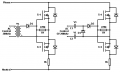
I had already seen the transformer coupling on the circuit to the left, but never the one on the right. Am I right in guessing that C1 and C2, together with D1 and D2 together form a voltage doubler, and so the Mosfet's gates are being triggered at 10V? ... I'm in doubt because, it almost looks like a voltage doubler... except that both nodes are decoupled through capacitors. Also, will this circuit work at much lower frequencies?

Gonna sim it and see what happens...
 

Thread Starter

cmartinez

Joined Jan 17, 2007
8,856
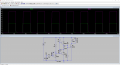
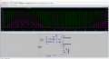
This is interesting. The gates are getting triggered at around 9V, which is good enough for most applications. But current seems to be flowing mainly in one direction only. Would that be because of D1?

upload_2018-4-23_22-12-52.png
 

Attachments

crutschow

Joined Mar 14, 2008
38,812
The circuit is designed to be an AC/DC SSR.
If you change R4 to 220kΩ as in the original schematic, then the gate-source voltage stays at a steady voltage with a small ripple, keeping the MOSFETs on.

D4 across the inductor shunts the current around the inductor for one polarity of the AC, as you observed.
You can't use a diode across an inductor in an AC circuit to suppress transients.

Note that those capacitors do not isolate this circuit from the AC line.
If you reduce the value of C1 and C2 to 200nF, that would limit any current to ground to <10mA which is generally considered to be safe.

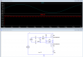
Below is the simulation with no D4 and the value of R4 changed.

upload_2018-4-23_20-59-13.png
 
Top