Newbie made is first PCB... help! :

Thread Starter

RARVA

Joined Jan 29, 2018
39
Hi guys, so i'm designing my first PCB... After many modifications I've come up with something I'm happy with.
But after educating myself around the web, i've come to realize that there are SO many conflicting rules and considerations... I'm just not sure of myself.
So, if anyone could be kind enough to give me feedback on the board I would appreciate.
The purpose of the board (beside making me learn in the process) is to control 64 leds independently... or more connecting another one in series. The chip used is going to be MAX7219.
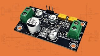
Some pics:

Nx64 Led Controller_TOP.jpg Nx64 Led Controller_BOTTOM.jpg

is first?""??" sorry for my english... newbie made his first PCB... :D
 
Last edited:

AlbertHall

Joined Jun 4, 2014
12,625
The link between the two sections of the ground plane doesn't seem to be actually connected to the ground plane at either end.
 

dendad

Joined Feb 20, 2016
4,637
It is generally not best practice to join a track to another with a "Y" connection. On my boards, if there is a join, and not a convenient pad there, I add one, like a feed through hole, just for the track join. And try to make the join at right angles, not sharp angles.
Your board will still work ok, but I try to make the layout look good too.
But well done! That is an excellent first effort!
 

joeyd999

Joined Jun 6, 2011
6,279
For the LED matrix area, run all horizontal traces on the solder side. Verticals on the component side. Remove ground plane under LEDs -- it serves no purpose.
 

AlbertHall

Joined Jun 4, 2014
12,625
It is generally not best practice to join a track to another with a "Y" connection. On my boards, if there is a join, and not a convenient pad there, I add one, like a feed through hole, just for the track join. And try to make the join at right angles, not sharp angles.
Your board will still work ok, but I try to make the layout look good too.
But well done! That is an excellent first effort!
Does this matter if the board is to be hand soldered?
 

Thread Starter

RARVA

Joined Jan 29, 2018
39
It is generally not best practice to join a track to another with a "Y" connection. On my boards, if there is a join, and not a convenient pad there, I add one, like a feed through hole, just for the track join. And try to make the join at right angles, not sharp angles.
Your board will still work ok, but I try to make the layout look good too.
But well done! That is an excellent first effort!
well, that's one doubt I was having, how do I make the distributing connections avoiding daisy chaining the components, as I understood, there would be a voltage drop at each connection the line pass thru. this was a try for a type of Source to Single Point. So it's ok to make right angles when distributing?
 

Thread Starter

RARVA

Joined Jan 29, 2018
39
For the LED matrix area, run all horizontal traces on the solder side. Verticals on the component side. Remove ground plane under LEDs -- it serves no purpose.
:) it was a compromise, in that way I lose the "direct path of the IC ground pads to the ground connector...
using the vias to connect upper and lower ground plane... was "upsetting me" but hey...
Will give it a go with suggested changes.
 

joeyd999

Joined Jun 6, 2011
6,279
:) it was a compromise, in that way I lose the "direct path of the IC ground pads to the ground connector...
using the vias to connect upper and lower ground plane... was "upsetting me" but hey...
Will give it a go with suggested changes.
For this design, it makes no difference either way. For the future, with denser designs, you should get used to making the traces of the top and bottom layers as perpendicular as possible. It makes routing far easier.
 

Thread Starter

RARVA

Joined Jan 29, 2018
39
Ok, what about now?
The only thing "itching me" is that the ground's IC doesn't make a straight path to the ground pin... :)Nx64 Led Controller_TOP2.jpg Nx64 Led Controller_BOTTOM2.jpg
 

Thread Starter

RARVA

Joined Jan 29, 2018
39
i hope this clarifies it...
View attachment 144671
Oh... that's nothing... it's just the connecting point of the plane... but has no effect if not used.
the vias was connecting the upper ground plane, thru a trace on top to the lower ground plane part.... but yes now I see that they where not connecting! ;) silly me... that's why a fresh look makes a difference! :D
 

Thread Starter

RARVA

Joined Jan 29, 2018
39
For this design, it makes no difference either way. For the future, with denser designs, you should get used to making the traces of the top and bottom layers as perpendicular as possible. It makes routing far easier.
hahaha... man... that's what I tried to do... thought I nailed it! ;) Guess not! :D
 

Thread Starter

RARVA

Joined Jan 29, 2018
39
I was trying to put all the signal traces on the bottom to be between the ground plane, as well trying not to cross the clock trace with other traces...
 

Thread Starter

RARVA

Joined Jan 29, 2018
39
I'm still confused about what people say, what I read, and my own logic reasoning about the subject. Can someone elaborate on the do's and don'ts of the examples bellow?How to.jpg
 

Thread Starter

RARVA

Joined Jan 29, 2018
39
Ok removed the fork solder pad... wasn't making much sense having to solder on a trace. Put a T fork and chamfered it.
Thanks guys for the help.

It's a go for production?
Nx64 Led Controller_OVERLAY.jpg Nx64 Led Controller_TOP3.jpg Nx64 Led Controller_BOTTOM3.jpg Nx64 top.png Nx64 bottom.png
 

dendad

Joined Feb 20, 2016
4,637
Can someone elaborate on the do's and don'ts of the examples bellow?
My vote is for "B".
Having a lot of traces fanning out from one pad as in most of the others is frowned upon in "professional" circles. One reason, according to the PCB expert that was running the Printed Circuit Technology course I attended years ago. It can lead to failures long term as it is harder to clean the etchant out of the sharp angles. In practice this may never be a trouble but I think it looks bad anyway.
Where you have the Vcc line coming out twice, I'd run one thicker track from left hand Vcc, C2, C1, Max7219, R1 right hand Vcc. Not having it loop over the top as you have shown. That way, as well as looking better I reckon, Vcc goes via the C2 and C1 caps so your bypassing would be better. Using as big as practical tracks for power is wise too, s'pecilly when you are going to daisy chain the boards. Remember, all the LED current will be flowing through the track.
Even to the extent of having the upper portion of the board a power plane. For power traces, bigger is better.
 
Top