Newbie made is first PCB... help! :

Thread Starter

RARVA

Joined Jan 29, 2018
39
My vote is for "B".
Having a lot of traces fanning out from one pad as in most of the others is frowned upon in "professional" circles. One reason, according to the PCB expert that was running the Printed Circuit Technology course I attended years ago. It can lead to failures long term as it is harder to clean the etchant out of the sharp angles. In practice this may never be a trouble but I think it looks bad anyway.
Where you have the Vcc line coming out twice, I'd run one thicker track from left hand Vcc, C2, C1, Max7219, R1 right hand Vcc. Not having it loop over the top as you have shown. That way, as well as looking better I reckon, Vcc goes via the C2 and C1 caps so your bypassing would be better. Using as big as practical tracks for power is wise too, s'pecilly when you are going to daisy chain the boards. Remember, all the LED current will be flowing through the track.
Even to the extent of having the upper portion of the board a power plane. For power traces, bigger is better.
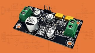
I already was using 32 mil trace for power trace, thought it was an overkill... but it depends how many will go in series... :) oh well since I have the space!
The specs of this IC says this two caps for bypassing, since if connecting another in series would have their own bypass caps also, my reasoning was to give a clean trace of power for the next in serie, with no voltage drop in between.
Are you saying something like this?:
Nx64 Led Controller_OVERLAY2.jpg
 

philba

Joined Aug 17, 2017
959
@dendad, Yeah, the R1 "jog" caught my eye too. I agree with your suggestions there. @RARVA, that looks a lot better.

By the way, those traces at 30 mils are wide enough to handle about 2A. It's always a good idea to do the analysis for your traces. Here's an easy to use tool. Typical copper is 1 oz. Look for a 10 degree rise max.
 

Thread Starter

RARVA

Joined Jan 29, 2018
39
@dendad, Yeah, the R1 "jog" caught my eye too. I agree with your suggestions there. @RARVA, that looks a lot better.

By the way, those traces at 30 mils are wide enough to handle about 2A. It's always a good idea to do the analysis for your traces. Here's an easy to use tool. Typical copper is 1 oz. Look for a 10 degree rise max.
:) I did research first... I swear! ;) That's the tool I used! I also downloaded PCBtoolkit (a bit complex for my knowledge skill though)
The board is 1oz FR4, 1.6mm TG150
I thought about using a power plane, but since my skill level is low, I tried not to add more complexity to the design... I really don't know what the iteraction of having power around signal traces would have, I did read that having a ground plane around signal lines was a good thing... but always read discouraging stuff about having a power plane on 2 layout PCBs.
 
You have Vcc on the left side of the board to Vcc on the right side of the board, make that trace horizontal. Then add a vertical perpendicular trace upwards to the resistor pad. part of the body of the resistor/one of the leads will be parallel to the small vertical trace.
 

Thread Starter

RARVA

Joined Jan 29, 2018
39
Nx64 Led Controller_OVERLAY2.jpg
You have Vcc on the left side of the board to Vcc on the right side of the board, make that trace horizontal. Then add a vertical perpendicular trace upwards to the resistor pad. part of the body of the resistor/one of the leads will be parallel to the small vertical trace.
? :) But it's already with a horizontal 48mil trace across vcc left and vcc right... and with 2 small vertical 32mil traces to the resistor ?
 

Thread Starter

RARVA

Joined Jan 29, 2018
39
I'd say pretty good. As long as long as the clearances are ok.
How could they not be? He's using 1980's design rules.
HAHAHA... Is that a bad thing or a good thing?! :)
In my friend circles no one knows nothing about this, so I really can't talk to anyone about it, and exchange ideias with ppl that have experience... that's mainly what I'm trying to learn here... I already digged (dug) a lot on the net trying to learn basic PCB rules... but... like someone out there put it: "give a project to 100 different engineers, and you'll get 100 different PCBs", can you point me to somewhere on the net with modern day design rules guidelines?
 

joeyd999

Joined Jun 6, 2011
5,283
Is that a bad thing or a good thing?!
I guess my point is that modern line/space requirements are significantly smaller than what you have presented. Your design is excellent for a first shot using DIPs. It'd be a no-go for a densely populated surface mount board.

Case in point: I typically use 7/5 line/space. 7 mil traces with 5 mil gaps between them. A reasonably modern fab house will do 5/5 or 4/4.

1 oz. copper is pretty darn conductive. Running 300 mA on a 10 mil trace is not at all unheard of.
 

Thread Starter

RARVA

Joined Jan 29, 2018
39
I guess my point is that modern line/space requirements are significantly smaller than what you have presented. Your design is excellent for a first shot using DIPs. It'd be a no-go for a densely populated surface mount board.

Case in point: I typically use 7/5 line/space. 7 mil traces with 5 mil gaps between them. A reasonably modern fab house will do 5/5 or 4/4.

1 oz. copper is pretty darn conductive. Running 300 mA on a 10 mil trace is not at all unheard of.
Ok ok, In fact I did the math, and I'm using larger traces than required for the amperage... lesson learn, stop being a chicken and wuss, and make it accordingly to the tech available on the 21 century!
On it! :D thanks for the push. ;)
 

philba

Joined Aug 17, 2017
959
I wouldn't worry about vias. Don't over do it but one per trace isn't going to cause any problems.

Old school tech? I wouldn't lose any sleep. The primary measure of a board isn't how it looks, it's whether it works - that's the high order bit here. You crossed that threshold a while ago.

Now, stop asking for advice and send it off to be made. You are so far away from their minimums, it would be a pathetic board house that would be challenged to make it.

And, start thinking of your next board. Surface mount parts rock.
 
Not what I had in mind in changing the orientation of the resistor, but it's probably better in the long run. i.e. easier to stuff.

I was suggesting keeping the same orientation of the resistor, but make the trace under one of the leads and/or part of the body

When thru-hole components are wave-soldered, there can also be a preferred orientation so other pads are not in front of the wave.
 

Thread Starter

RARVA

Joined Jan 29, 2018
39
Not what I had in mind in changing the orientation of the resistor, but it's probably better in the long run. i.e. easier to stuff.

I was suggesting keeping the same orientation of the resistor, but make the trace under one of the leads and/or part of the body

When thru-hole components are wave-soldered, there can also be a preferred orientation so other pads are not in front of the wave.
ah... it's going to be hand soldered... but it's always good to be aware of wave-soldered considerations... although I'm not there yet! :D
 

Thread Starter

RARVA

Joined Jan 29, 2018
39
Ok, this is the smallest physically board I could make.
It's started out at 30€ for 3 boards... this version is 10€ for 3 boards... so at least it's something.
I used smaller traces considering the current used.
Ground plane on the bottom, power plane on top.
Stayed 50% on the safe zone considering the manufacturer capabilities (4/4). I'm doing 8/8.
The only thing I'm not sure, do I leave unconnected copper areas?
Nx64 Led Controller_TOP5.jpg Nx64 Led Controller_BOTTOM5.jpg Nx64 Led Controller_OVERLAY5.jpg
Did I push it too far? or it's a go?
 
Top