Need help to light up 8 LEDs with different color

Thread Starter

jenovauh

Joined Jul 4, 2013
246
I tried to assemble the circuit a couple of time but I could not get it working.

Bernard could you do me a very last favor and draw everything clearly you said in the post with the latest modification and parts on a picture and I work on there. I believe I already had the parts you need me to use unless you have new parts in your new modification. Thanks.
 

Bernard

Joined Aug 7, 2008
5,784
Before connecting Day Night ckt, did the battery pickup the load as SP lost the sun? I wondered how the B-B output behaved as SP dropped power. What P ch FET are you using?
You may wish to use a pot for R2, R3 to find the best day -night transferr; any thing from 10k to 100k should be fine, but add a 1k between SP & top of pot so that SP cannot be inavertantly conneced to pin 2. Pot tap goes to pin 2. Wish you luck.
 

Attachments

Thread Starter

jenovauh

Joined Jul 4, 2013
246
Like right now, it is going to start raining soon. I check the SP output only have 1.2-1.4V and B-B output have 40-50mV. I am using the the SMD FDS9435A.

To find the best day for night transfer, what should I achieve then I can consider I had done it correctly? Example the battery is supply power to the LED circuit? Or SP is charging the battery when SP have extra current? Sorry I am a bit confused here.
 

Thread Starter

jenovauh

Joined Jul 4, 2013
246
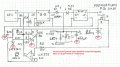
Hi Tracecom, are you able to help to draw out the attached circuit as I am not sure if I had assembled them correctly. Could be the reason why it did not work. I had 4 red circle in the picture which I am not sure. Thanks

1. R2 pot connection for pin 1, 2 and 3 (using 50k pot as mentioned on post #222 to use anything from 10k to 100K pot)
2. R3 pot connection for pin 1, 2 and 3 (using 50k pot as mentioned on post #222 to use anything from 10k to 100K pot)
3. LM336, never use one before and are not be sure which pin to connect to in the circuit. I try to google for reference but cant seem to find them.
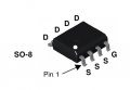
4. FDS9435A have 8 pin but the drawing only show D G S, does that mean I can use any pin 5 to 8 for D, pin 1 to 3 for S and pin 4 for G?
 

Attachments

Thread Starter

jenovauh

Joined Jul 4, 2013
246
Hello,

I have attached the datasheet of the LM336.
If you can not find a LM336 a TL431 can also be used.

Bertus
Hi Bertus, thanks for the data sheet, I found the datasheet. What I am not sure is that the adj pin need to be connected to pin 3 or pin 5 of LM393? And actually what does this LM336 do exactly in the circuit? Fix the voltage in the circuit to 2.5V and why need to do that?
 

Thread Starter

jenovauh

Joined Jul 4, 2013
246
jenovauh,
A picture of the breadboard and a snip of the schematic are attached for your review. I suggest that you compare them in detail. If you want to PM your e-mail address to me, I will sent you a copy of the DipTrace schematic file.
Hi Tracecom, I message you twice on my email to get the Diptrace file. Did you receive my message?
 

bertus

Joined Apr 5, 2008
22,960
Hello,

In case of the LM336 the adj pin does not need to be connected.
The LM336 provides a fixed voltage used as reference for the LM393.
This is needed as the battery voltage may vary.
The LM336 is connected to both pin 3 and 5.

Bertus
 

Thread Starter

jenovauh

Joined Jul 4, 2013
246
In other words, only the V- and V+ are used in the drawing? V- to pin 3 and V+ to pin 5? But the LM336 in the drawing shows the V- to the ground symbol. I do not know if I am stupid or what. I really could not figure out on the drawing at all. And I believe I might had made a lot of mistake here and there when I am try to follow the drawing to assemble the circuit. Sigh. I do not know, I just find it very hard to follow the drawing without clear labels and indicators.
 

bertus

Joined Apr 5, 2008
22,960
Hello,

All ground marks are part of the V- connections and should be connected together.


As for the mosfet.
You can connect all drains on one side together
and source connections on the other side together.


It is the best to have a mounting plane for cooling the mosfet.
In the datasheet there are some examples given for mouning planes with their colling capacity:


Bertus
 

Attachments

Thread Starter

jenovauh

Joined Jul 4, 2013
246
Hi bertus, I had found those picture you posted here. I don't understand how to connect LM336 to both pin 3 and pin5 of LM393.
 

Bernard

Joined Aug 7, 2008
5,784
On recent post, can you connect pins 3 & 5 together? If so connect LM336V cathode to either pin 3 0r 5. On drawing NC stands for no connection, K for cathode + output, A for anode, - out or ground.
On New drawing, shows how R2 & R3 wewr converted to R2, 1k, & R3 to a 50k pot
You surprised me in using a SM FET. On mine ,I attached a strip of self stick copper foil to a 5 X 6 piece of thin aluminum, .15 mm, then soldered all drains to edge of copper along with a 5 cm red wire suitable for solderless bread board. Sources connected to a black wire, single gate pin connected to a green wire. In this use as a switch, power disipation will be low, around 15 mW, so just wires will be enough of a heat sink.
 

Attachments

tracecom

Joined Apr 16, 2010
3,944
On New drawing, shows how R2 & R3 wewr converted to R2, 1k, & R3 to a 50k pot.
Bernard,

I am going to try to get the entire schematic into DipTrace; attached is how I understand the comparator section. Is it correct, and if so, where does pin 7 of the LM393 connect?

ETA: Correction made to schematic, and attached to post 241; attachment deleted from this post to avoid confusion.
 
Last edited:

Thread Starter

jenovauh

Joined Jul 4, 2013
246
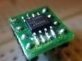
I am using the SMD FDS9435A by soldering onto SOP8 to DIP8 adapter.

Tracecom, thank you so much for helping to draw the schematic into Diptrace.
 

Attachments

Last edited:

tracecom

Joined Apr 16, 2010
3,944
Bernard,

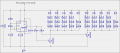
Attached is how I understand the latest versions of the 555 and LED sections. By my calculations, the duty cycle is 60.66% on at 2.36 kHz. Are my calculations and schematic correct?


What is the expected voltage at the junction of D1 and D2 from the buck regulator and the buck boost regulator? What should be the R values for R5 through R14?

Thanks.
 

Attachments

Last edited:

Bernard

Joined Aug 7, 2008
5,784
Bottom of pot,R3 should not go to ground but as in post 222 or 230, pin 7. Nice schematic. What was the time of day & weather conditions when you measured SP @ 1.4 V? Assuming that it was day with heavy cloud cover, then the LED's should have been operating on battery? Should we call SP switchover from cloudy to night as 1.25 V, @ night less than .5 V? Let us leave it as is for now & fine tune it later.
Attempt at explaning day- night operation: Starting late after noon, clear sky, SP putting out about 11V loaded, B-B output, D1 cathode @ 10V. Comp. A, pin 2 is now higher than pin 3 @ 2.5V, so pin 1 is low, turning FET on. Battery V is reduced to 9.5V so it does not power LED's, but is ready if B-B falls below 9.5V. Say a cloud passes over, SP falls to 3V, B-B falls below 9.5V, battery now supplies power to LED's. Night falls, SP falls below 2.5V, Comp A reverses output as pin 3 is now higher than pin 2; battery now disconnected, Comp B pin 6 is now higher than Ref V of 2.5V so pin 7 goes low grounding bottom of pot. Pin 2 is now pulled down more so that when sun comes up SP must put out around 3 V, adjuistable, before the battery is again connected.
 
Top