Need help to light up 8 LEDs with different color

tracecom

Joined Apr 16, 2010
3,944
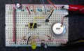
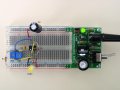
Attached is a photo of a breadboard using a 555. It is not your circuit, but it shows how to place the capacitors. C3 is a .1uF cap that goes from pin 1 to pin 8 of the 555; there is no polarity, so it can go in either way. C4 is a 10uF cap that is across the power bus; it is polarized and the negative side of the capacitor must go to the ground and the positive side must go to +VDC.

Notice that, electrically, the two caps are in the same exact place in the circuit, i.e., from ground to +VDC, but physically, they are in different locations on the breadboard. That is because they perform two different functions. C3 is to protect the 555 from noise on the power bus. C4 is to suppress the noise that the 555 puts onto the power bus. It is not absolutely required that they be arranged this way, but it is most important that C3 be physically very close to pins 1 and 8 of the 555.
 

Attachments

Thread Starter

jenovauh

Joined Jul 4, 2013
246
Attached is a photo of a breadboard using a 555. It is not your circuit, but it shows how to place the capacitors. C3 is a .1uF cap that goes from pin 1 to pin 8 of the 555; there is no polarity, so it can go in either way. C4 is a 10uF cap that is across the power bus; it is polarized and the negative side of the capacitor must go to the ground and the positive side must go to +VDC.

Notice that, electrically, the two caps are in the same exact place in the circuit, i.e., from ground to +VDC, but physically, they are in different locations on the breadboard. That is because they perform two different functions. C3 is to protect the 555 from noise on the power bus. C4 is to suppress the noise that the 555 puts onto the power bus. It is not absolutely required that they be arranged this way, but it is most important that C3 be physically very close to pins 1 and 8 of the 555.
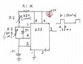
Thanks for the detail explanation. I did mine exactly on your picture on C3 before you did the post. I am just confused with the diagram on post #196 which I had circled in red and receiving the replied from you guys telling me to put the capacitor from pin 1 to pin 8. The diagram itself did not show a connection between pin 1 and pin8. Which makes me to think that this circuit now have 3 Capacitors? Or it is just my understanding on the circuit drawing is really that bad.
 

tracecom

Joined Apr 16, 2010
3,944
The red circled cap in post 196 is the same cap as C3 in my photo. It goes from pin 8 to ground, but it should be located from pin 8 to pin 1. Electrically, they are both in the same place in the circuit, but C3 is in the correct physical location. Look in the photo and see that C3 goes from pin 8 to pin 1 (pin 1 has a white dot by it.) Then, notice that pin 1 has a black wire going to the ground bus on the breadboard. So C3 goes from pin 8 to pin 1, but because pin 1 is connected to ground, C3 electrically is connected from pin 8 to ground.

I know that you research electronic components and circuits, and are learning a lot. I think that you would understand more if you began to draw your own schematics. Drawing schematics helps to learn the relationship between electrical locations and physical locations of components. If you are building your grow light as a one-time effort, you probably don't need to bother with drawing schematics, but if you want to continue in electronics, I think it would help.

There are lots of software packages for drawing schematics; some are free. I use DipTrace, and have the version that costs about $150, but there is a free version available.
 
Last edited:

Thread Starter

jenovauh

Joined Jul 4, 2013
246
The red circled cap in post 196 is the same cap as C3 in my photo. It goes from pin 8 to ground, but it should be located from pin 8 to pin 1. Electrically, they are both in the same place in the circuit, but C3 is in the correct physical location. Look in the photo and see that C3 goes from pin 8 to pin 1 (pin 1 has a white dot by it.) Then, notice that pin 1 has a black wire going to the ground bus on the breadboard. So C3 goes from pin 8 to pin 1, but because pin 1 is connected to ground, C3 electrically is connected from pin 8 to ground.

I know that you research electronic components and circuits, and are learning a lot. I think that you would understand more if you began to draw your own schematics. Drawing schematics helps to learn the relationship between electrical locations and physical locations of components. If you are building your grow light as a one-time effort, you probably don't need to bother with drawing schematics, but if you want to continue in electronics, I think it would help.

There are lots of software packages for drawing schematics; some are free. I use DipTrace, and have the version that costs about $150, but there is a free version available.
I understood what you mean but some more could not mentally map the connecting between them lol. Yes I think you are right, I need to start learning how to draw schematics and DIY my own PCB board for the grow light. Done my research and got the required material to DIY my own PCB too.

I even bought a desk oscilloscope but don't really know how to use it lol. I was testing on the circuit to find out if it got pulse frequency above 720hz but could not seem to get it. Can you give me some pointers on where should I tap on the circuit to check for the pulse frequency readings?

My interest in electronic is to make energy saving lights for the plant for now, maybe when I can design my own light I will try something else. :)
 

Thread Starter

jenovauh

Joined Jul 4, 2013
246
4. 4017 demise. What do plants want, twinkling light or full light seperated by full dark & what ratio of light to dark. Using4017 itispart of each , half of the light for half of the time; 555 gives full light with adjustsble ratio of light to dark. Your choice.
1. B-B is boost & buck, B is buck only. I believe that you have one of each.
2. SP & B-B puts out 10 V, 12V battery & B put out 9.5V, just low enough to allow the two sources to be " ORd " via 2 1n4001's io LEDs. As sun lowers, SP output will finally drop out of regulation & V will fall. When both output Vs are equal , both will supply power, a further drop in SP V, battery takes over untill sunset is determined.
3. Any 1n4XXX diode is OK if over 50V, inc. 1N4001.
Hi Bernard, I had done and tested the circuit for days and they seem doing alright. Are you able to advise on the battery charging portion? Thanks.
 

Bernard

Joined Aug 7, 2008
5,784
jenovauh, your schrmatic is prettier than my drawing,but you need a few changes to make it work. Best if you reviewed it & find problems, but here is a clew: there is no input to trigger, pin 6 will always be high, so 7 always low, pin 3 always low. Will be back in evening.
 

Thread Starter

jenovauh

Joined Jul 4, 2013
246
jenovauh, your schrmatic is prettier than my drawing,but you need a few changes to make it work. Best if you reviewed it & find problems, but here is a clew: there is no input to trigger, pin 6 will always be high, so 7 always low, pin 3 always low. Will be back in evening.
Hi Bernard, are you able to give me some advises on how to check the above mentioned problems? I have no clue how to do that. Thanks.
 

Bernard

Joined Aug 7, 2008
5,784
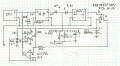
#1 origional print, #2 new print. Review #1 & note that all timing components are in series, R1- R2- R3- C1. How many connections to top of R1? 4, right? Vcc, pin 8, pin 4, + side of C2. Are the same connections made on #2? Yes. R1- R2 connection? No connections. Ccompare with #2,= Faulty connection, remove. R2- R3 connection, D1 anode, pin7. Compare with #2. pin 7=OK, D1 misplaced, move top of D3 & anode , D1 to pin7. D3-C1 junction? D1 cathode, pin 2 & pin 6 Compare to #2. OK except no connection to pin 2. Connect pin 2 & 6. In addition you can compare both #1 & #2 pin by pin to see if they all go to same place.
If using fixed value Rs, R1 is not needed.
As Bertus noted, we need C3 on VCC, it was at one time on LED ckt but was lost on post 190. Now power is pulsed on or off so a larger C is used, up to 1000 μF, + to VCC.
To me the over use of the Quote is just a waste of memory, Sometimes what I say is not worth repeating.
 
Last edited:

Thread Starter

jenovauh

Joined Jul 4, 2013
246
Hi Bernard, I still cannot confirm if my schematic drawing is correct as per your design. No drawing to refer to and also advise added in for correction. I am trying my very best to understand and visualize what everyone is trying to tell me here. Are you able to advise where is D3 and C3? I hope you understand without a drawing and some numbers of typo when explaining I will make mistake as well. The LED circuit I did not draw because I have no problem with that and it is not lost.

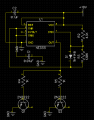
Yes I am using fixed resistor as you mentioned that it should get around 750hz. I will remove R1 1k resistor base on your advise. And also corrected what you have mentioned on post #209. I have attached the new drawing with the the 2 X 2N2222 drivers except LEDs. I hope you can correct the drawing if I had done it wrongly. Thanks.
 

Attachments

Last edited:

tracecom

Joined Apr 16, 2010
3,944
jenovauh,

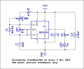
I have redrawn the schematic in DipTrace and also have built the circuit on a breadboard. The circuit works well.

A picture of the breadboard and a snip of the schematic are attached for your review. I suggest that you compare them in detail. If you want to PM your e-mail address to me, I will sent you a copy of the DipTrace schematic file.

I don't have any more time this morning, but will try to answer any questions later today.

@Bernard,

I don't mean to interfere, but am trying to help. Just say the word, and I'll butt out. :)
 

Attachments

Last edited:

Bernard

Joined Aug 7, 2008
5,784
tracecom, we need all the help we can get, thanks; ' like your layout better than jenovauh's as it is functionall easier to see 555 operation.
D3 is really D1; C3 described by Bertus, post 199, also post 209, just up value to 500 to 1000μF, whatever you have. Location not critical as long as C+ goes to VCC & C- goes to ground.
New schematic should work fine, just add C3.
 

Thread Starter

jenovauh

Joined Jul 4, 2013
246
Hi tracecom, thanks for the help and I will pm you for the file.

Hi Bernard, new schematic referring to my drawing? C2 is actually the capacitor Bertus had mentioned when I circled in red on your previous drawings. I really don't know what is what now. Where to place another capacitor where there is no where to put it.
 

Bernard

Joined Aug 7, 2008
5,784
Next step: Day - Night control. If you still have not received the 2.5V ref IC, we will go back to using a red LED, 2V. As evening approaches, LED ckt is most likely running on battery but there is still some V from SP. As long as SP puts out more than 2V ref, comp. -1, out will be low keeping FET on, battery connected. When SP falls below 2V, comp switches to open collector, putting Vcc on G, batt. disconnected. second half of comp is an inverter. When pin 6 goes high, pin 7 goes low, pulling pin 2 a bit lower so that when SP V goes back above 2V , it must continue up to about 3V to prevent spurious activations. Must run.
 

Attachments

Thread Starter

jenovauh

Joined Jul 4, 2013
246
Hi Bernard, I had received the 2.5v ref IC awhile ago. Anyway I had studied the circuit and noticed that C3 have no value on it. I will try to draw the circuit on schematic and try to fix them up together and try on this coming weekend.
 

tracecom

Joined Apr 16, 2010
3,944
C3 is the same C3 that was discussed in the last few posts. Bernard said to make it about 500-1000μF, and that the value was not critical, so I put it in the schematic at 470μF. It is just a filter cap.
 

Bernard

Joined Aug 7, 2008
5,784
Go back to post # 138 for LM336Z connections, yes change 1K to 4.7 k.
Maybe tracecom can offer a better P ch FET for surface mount one shown. Found that I have an IRF9540 & IRF9540, P ch. FET, 200V, 11A in TO220 pkg; a little over rated for present load of 200 mA.
On bread board 12k & 19k are a 32k multi turn pot, might make 19k a standard value of 20k & raise 12k to 15k to increase hysteresis a bit.
Note that the comparator is alyays powered by battery.
In day, pin 7 is high, ie open allowing full SP V on pin2 so it may be best if pin 2 is clamped at + battery by adding a 1N4148 diode, anode to pin 2, cathode to pin8, + battery.
 

tracecom

Joined Apr 16, 2010
3,944
The BS250 is rated for 250mA max. I would probably use two of those in parallel, but that is heavily influenced by the fact that I have some in hand.
 
Top