Facebook
 Google
 GitHub
 Linkedin
Hi everybody! Hope you're good! ")
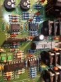
I'm strugglin since some days on that nice muscial tool. I've replaced some faulty switches. Replaced them with new one from Mouser.
Sadly I've managed to hurt some VIAS connecting both side of the board. Luckilly enough this is just 2 layer board (top/bottom) so I can manage to restore the connection easily.
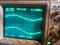
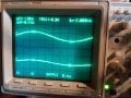
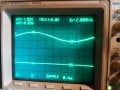
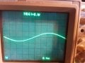
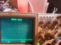
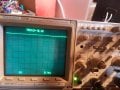
I already found one problem quite faste by signal tracing with my oscilloscope and "beeping" some traces and fixed it. So sound is back on both channels. There still some problems and yesterdy, after overloading the input by accident, I apparently killed one of it's channel.
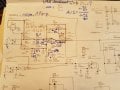
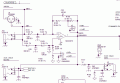
So now I need to understand exactly what went wrong and I wanna understand the schematic, but for this I need some help. I've learned much about eletricity but It's some years ago and I lack experience.
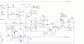
So I drawed this for you: (the second unmarked "+4/-10" switch is SW2C)!
EDIT: I also have forgotten to mention +/- of the opamp. So this is an inverting one, so the upper pin is - and the lower +

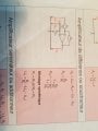
So I'd like to know what my output will be if at Tx input is 1V. What resistors to take into account for the gain calculation?
As this is balanced audio input IN1- will always be the opposite of IN1+! So for 1V IN1- = -1V
Why are there to different grounds? What's the effet they're looking for?
So my analysis made me thinking this is also a band-pass filter because of C52 and C51 Right?
By the way, original schematic can be found under goolgle with "dbx1066 schem" query if you're interested.
Any help very much appreciated!
Cheers,
David
I'm strugglin since some days on that nice muscial tool. I've replaced some faulty switches. Replaced them with new one from Mouser.
Sadly I've managed to hurt some VIAS connecting both side of the board. Luckilly enough this is just 2 layer board (top/bottom) so I can manage to restore the connection easily.
I already found one problem quite faste by signal tracing with my oscilloscope and "beeping" some traces and fixed it. So sound is back on both channels. There still some problems and yesterdy, after overloading the input by accident, I apparently killed one of it's channel.
So now I need to understand exactly what went wrong and I wanna understand the schematic, but for this I need some help. I've learned much about eletricity but It's some years ago and I lack experience.
So I drawed this for you: (the second unmarked "+4/-10" switch is SW2C)!
EDIT: I also have forgotten to mention +/- of the opamp. So this is an inverting one, so the upper pin is - and the lower +
So I'd like to know what my output will be if at Tx input is 1V. What resistors to take into account for the gain calculation?
As this is balanced audio input IN1- will always be the opposite of IN1+! So for 1V IN1- = -1V
Why are there to different grounds? What's the effet they're looking for?
So my analysis made me thinking this is also a band-pass filter because of C52 and C51 Right?
By the way, original schematic can be found under goolgle with "dbx1066 schem" query if you're interested.
Any help very much appreciated!
Cheers,
David