Just some general questions about remaking something from the past

Status
Not open for further replies.

Thread Starter

Berzerker

Joined Jul 29, 2018
623
bertz said:
You cant just move the IC without moving the hole pattern.
Have you created a component called TDA7396 and stored it in your custom component library?
Have you created a pattern for the TDA7396 and stored it in your custom pattern library?
Have you linked your component to the pattern?
Yes I have all that. The other 11 holes are to connect wires to so I can lay the TDA7396 down flat on the heat plate. If not I would have to bend the plate down to connect it to which cost more money. It's the way I'm designing it. Trying to get by with a flat plate I guess is what I'm saying. This is a separate PCB to connect to the main PCB.
bertz said:
The TDA 7396 has 11 pins. You are showing 22 pins. What's up with those horizontal bars?
I didn't hit auto route, I done it manually. I assumed when you send your PCB to be made you didn't have the component pattern in it (?)
It's a board with holes in it right ?
 
Last edited:
ebeowulf17

Joined Aug 12, 2014
3,307
Here's better look at everything
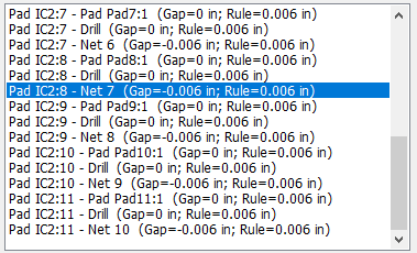
....... error list...…...

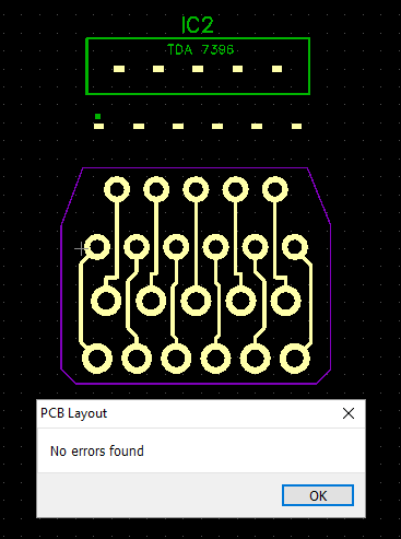
Now if I move the IC I get this
I think l see where you've gone wrong.

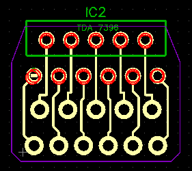
It looks like you designed a pattern that matches the part pins as closely as possible, then you separately put 11 holes in your PCB to match up with the pins, then you test fit by putting the pattern with pins in the same spot as the holes. Correct me if I'm wrong, of course.

What you're intended to do is design a pattern of pads/holes that represent what the part NEEDS, not what the part IS. There shouldn't be anything that looks like the rectangular pins anywhere in your files. Your pattern for TDA7396 should be the arrangement of 11 holes/pads, along with any silkscreen markings.

What you've got in the lower part of the lower image (with IC2 moved away from the 22 holes) is pretty close to what ultimately need to end up with. You've got the 22 holes you want, and you've got them connected the way you want, and you've got no errors.

The problem is that you've got IC2 floating about as its own entity, not connected to any traces. Strictly speaking, you could just delete IC2 from that layout and have the PCB file you need... but it wouldn't tie in to your schematic file in any useful way.

What you probably really need to do is:
  1. Modify your pattern for TDA7396 such that it has holes/pads instead of pins.
  2. Delete the 11 extra holes on the top half of your board layout.
  3. Connect your traces from the bottom pads to your updated TDA7396 pattern pads.
 

Thread Starter

Berzerker

Joined Jul 29, 2018
623
Thanks ebeowulf. I won't quote the post (#402) above ebeowulf to save room on the page but your right. I did put ratlines from the component itself at first to the bottom 11 holes/pins and hit autoroute, I came up with the 50 or 60 errors. even the bottom holes had errors and there isn't a component that goes in them. I'm kinda using it like a terminal because there are going to be three PCB boards on it. The amplifier and two DC converters for the IC's power inputs. But after stopping and thinking more on the radio itself last night don't they all have a low voltage output to give a signal to an amp to kick it out of stand-by or the mute stage "a remote turn on wire" I think it's called. If this is 5V or so then I won't need one of those converters. I will do what you say and show you the results.
 

ebeowulf17

Joined Aug 12, 2014
3,307
Thanks ebeowulf. I won't quote the post (#402) above ebeowulf to save room on the page but your right. I did put ratlines from the component itself at first to the bottom 11 holes/pins and hit autoroute, I came up with the 50 or 60 errors. even the bottom holes had errors and there isn't a component that goes in them. I'm kinda using it like a terminal because there are going to be three PCB boards on it. The amplifier and two DC converters for the IC's power inputs. But after stopping and thinking more on the radio itself last night don't they all have a low voltage output to give a signal to an amp to kick it out of stand-by or the mute stage "a remote turn on wire" I think it's called. If this is 5V or so then I won't need one of those converters. I will do what you say and show you the results.
Cool, good luck on the pin rearranging.

As for the remote turn on wire, I'm pretty sure that it can't deliver any significant power. I think those outputs are literally only meant to deliver a signal to trigger other devices, but not to power them.

*** EDIT: I checked the specs on the new stereo I just installed, and it can provide up to 0.4A, so it can deliver *some* power, but not nearly enough for your amplification needs.
 

bertz

Joined Nov 11, 2013
327
Thanks ebeowulf. I won't quote the post (#402) above ebeowulf to save room on the page but your right. I did put ratlines from the component itself at first to the bottom 11 holes/pins and hit autoroute, I came up with the 50 or 60 errors. even the bottom holes had errors and there isn't a component that goes in them. I'm kinda using it like a terminal because there are going to be three PCB boards on it. The amplifier and two DC converters for the IC's power inputs. But after stopping and thinking more on the radio itself last night don't they all have a low voltage output to give a signal to an amp to kick it out of stand-by or the mute stage "a remote turn on wire" I think it's called. If this is 5V or so then I won't need one of those converters. I will do what you say and show you the results.
The datasheet tells you this is made by ST Micro. Go to the "Component" module and select ST Micro and scroll down the list of components. Very often you will find the exact component. Unfortunately in this case they don't list the TDA7396. But if you scroll up and down you can find a component that has a pattern match that you need (Multiwatt 11). In this case a TDA8174. Select it and save it to your custom folder. Now you can edit the pins according to the data sheet and you have an exact pattern match.
 

Thread Starter

Berzerker

Joined Jul 29, 2018
623
OK I found them. But I had already made my component up and from what I understood it was ok. My pattern was already made (by me)
and it was correct as far as dimensions. all I need to do is make the pins like I would want them on the board and just attach that pattern to my component right? The only thing different in the TDA8174 and mine was the dimension from the back to the pin centers and my pattern is already correct. So at least I know how to do a pattern from scratch if need be. I had everything pretty close except my solder pads were .093 and it's were .075 (and I was just guessing). I don't think a little bigger pad to solder to is a bad thing.
 

shortbus

Joined Sep 30, 2009
10,049
he datasheet tells you this is made by ST Micro. Go to the "Component" module and select ST Micro and scroll down the list of components. Very often you will find the exact component. Unfortunately in this case they don't list the TDA7396. But if you scroll up and down you can find a component that has a pattern match that you need (Multiwatt 11). In this case a TDA8174. Select it and save it to your custom folder. Now you can edit the pins according to the data sheet and you have an exact pattern match.
For some reason he doesn't want to do it easy. I told him to do the same thing pages ago.
 

Thread Starter

Berzerker

Joined Jul 29, 2018
623
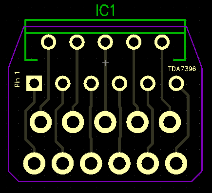
OK went back an redone it. Is this right?


shortbus said:
For some reason he doesn't want to do it easy. I told him to do the same thing pages ago.
But you have to understand all those numbers in Diptrace are confusing at first. and yes I'm hard headed I get it from my Dad.
Now all I have to do is make sure all the correct layers are there and are right.
 
Last edited:

ebeowulf17

Joined Aug 12, 2014
3,307
OK went back an redone it. Is this right?


But you have to understand all those numbers in Diptrace are confusing at first. and yes I'm hard headed I get it from my Dad.
Now all I have to do is make sure all the correct layers are there and are right.
Are you getting any DRC errors? If not, that's a good start.

If you drag IC1 around, do the top 11 holes move around with it? (They should!)

It looks like part of your silkscreen goes outside of your board outline. You'll either need to scoot components in, or make your outline bigger.

That's all I see for now.
 

Thread Starter

Berzerker

Joined Jul 29, 2018
623
No errors ebeowulf. yes if I move the IC the pattern goes with it. the DRC should tell me if there's something outside the silk screen right?
But I am still trying to tell the difference in silk screen, bottom and top layers, top and bottom masks....etc. Reading on that now.
Edit: are you talking about where it says IC1 and the end of the IC itself?
 
Last edited:

ebeowulf17

Joined Aug 12, 2014
3,307
No errors ebeowulf. yes if I move the IC the pattern goes with it. the DRC should tell me if there's something outside the silk screen right?
But I am still trying to tell the difference in silk screen, bottom and top layers, top and bottom masks....etc. Reading on that now.
Edit: are you talking about where it says IC1 and the end of the IC itself?
Yes, the stuff in green. I'm assuming that's on your silkscreen layer, which is the layer of stuff that will get printed on the board.

If it is silkscreen, obviously it can't go beyond (or even get too close to) the edge of the board. I don't remember if DRC checks silkscreen or not.
 

Thread Starter

Berzerker

Joined Jul 29, 2018
623
ebeowulf said:
Yes, the stuff in green. I'm assuming that's on your silkscreen layer, which is the layer of stuff that will get printed on the board.
If it is silkscreen, obviously it can't go beyond (or even get too close to) the edge of the board. I don't remember if DRC checks silkscreen or not.
No that's the IC outline or what I placed in the pattern editor to identify it to me (the IC1 part). So it also will get printed on the PCB too? I'm learning but I guess I still don't have some things right. Then I will have to redo my pattern and place the green inside my board outline because I don't want the PCB to hold my IC from being bolted down. The board outline is what I need to go by to get what I want.
Edit: I did have to go to wally world today and found a cheap radio to use to test everything with $17.00. Says 120 Watts but don't tell AG he'll probably go off about the 120 watts thing.
 
Last edited:

ebeowulf17

Joined Aug 12, 2014
3,307
No that's the IC outline or what I placed in the pattern editor to identify it to me (the IC1 part). So it also will get printed on the PCB too?
No way for me to tell from here. It certainly *looks* like stuff that goes on the silkscreen layer, but you've done everything yourself from scratch, and you already said earlier that you've customized the display colors, so all I can do is guess.

Is it on the silkscreen layer? Try turning your silkscreen layers on and off. Does it go away? If so, it's on your silkscreen layer. Anything on your silkscreen layer will get printed in ink onto your board, so it needs to land within your board outline.

But for all I know, you've made one of your assembly layers green, and that's what we're seeing in your screenshots. Assembly layers are for reference only, a useful way of communicating assembly notes or design intent. They don't get printed anywhere, and they don't take any physical form when the board is made, so you can put anything you want there.
 

Thread Starter

Berzerker

Joined Jul 29, 2018
623
ebeowulf said:
Is it on the silkscreen layer? Try turning your silkscreen layers on and off. Does it go away? If so, it's on your silkscreen layer. Anything on your silkscreen layer will get printed in ink onto your board, so it needs to land within your board outline.
You must be psychic I was just reading on how to tell what's on it. and when I turned it on nothing changed. My phone dings and I check and it's your answer. Ok now If I turn it on and place text in it while the silk layer is on that's what will get printed on that layer ? If I turn on another layer and make a change that's what happens on that layer then right ? Then it's a lot like AutoCad, you work in layers. Do I have to turn all the other layers off while I make changes in that layer ? How many layers do I need to worry about on a single sided PCB ? There are 11 in the right hand screen. Only 2 show anything in them.
 

shortbus

Joined Sep 30, 2009
10,049
Think there needs to be some clarification here.

The other 11 holes are to connect wires to so I can lay the TDA7396 down flat on the heat plate. If not I would have to bend the plate down to connect it to which cost more money. It's the way I'm designing it. Trying to get by with a flat plate I guess is what I'm saying. This is a separate PCB to connect to the main PCB.
So your making a separate PCB that will hold the IC and soldering wires from that to a main PCB?? Or what you showing as IC1 will not actually be in the place you're showing? If either of those things are true you wouldn't show both the separate parts on the main PCB. Only parts mounted to the PCB should be shown on any one PCB.

If your meaning "heat sink" instead of "hot plate", Those are better off up in the air flow. The type of IC you showed earlier is usually mounted up right and the heat sink is mounted to it and hot melt glued to the PCB. That is why they make it with the pins inline with the body of the IC.

How many layers do I need to worry about on a single sided PCB ?
Unless I'm mistaken, on a single sided PCB there is only one layer. The silk screen and solder mask are separate from the PCB, though they can be shown to make sure they are in the correct place. But should be turned off otherwise.
 

ebeowulf17

Joined Aug 12, 2014
3,307
Unless I'm mistaken, on a single sided PCB there is only one layer.
I think the word layer is used to mean a lot of different things in different contexts.

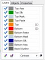
There's only one copper layer on a single sided PCB, but DipTrace also refers to solder mask, silkscreen, etc. as layers:
2B35EA10-27C1-42C4-A48C-ADE39BA80879.jpeg
 

MisterBill2

Joined Jan 23, 2018
27,977
First, Osborn, or Osborne, Transformer company was located in the city of Detroit, Michigan, at least when I last contacted them. BUT that was many years ago. (15) Things may have changed. There are still articles on winding your own transformers, and for this kind of audio amplifier that should not be that hard to create. IF the input (driver) transformers really had only four leads, then there has to be more external circuitry somehow. But that does not matter if you are doing a rework of the original design, you can have a center tapped secondary winding and simplify the whole system, plus making it easier to adjust and check. The size will determine the power handling ability of the transformer, since you do not want to drive the core into magnetic saturation, or even into that part of the curve. So you will need to learn a little about magnetization and amp-turns. Since you have decided on a power level and a supply voltage you can know the maximum current, and then calculate the effective driving impedance. And since you have picked the load impedance, now you can calculate the turns ratio. Also, given the peak current, you can select a wire size to use, although I suggest #18 based on experience. And it is easier to work with.
If your library has it, you can study the chapter on audio transformer design in the "Radiotron Designers Handbook", Langford Smith, Author. It covers tube circuits, but the principles hold for transistors as well.
I hope that this rambling discourse has been of some value, or at least of some interest.
 

ebeowulf17

Joined Aug 12, 2014
3,307
Ok now If I turn it on and place text in it while the silk layer is on that's what will get printed on that layer ? If I turn on another layer and make a change that's what happens on that layer then right ? Then it's a lot like AutoCad, you work in layers.
No, the layer tab is used to control which layers are visible, but does not determine which layer(s) you're working on. The resulting layers may be similar to AutoCad, but the ways you apply things to them are significantly different.

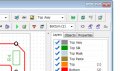
When you place components or through hole pads, they have data on numerous layers. When you draw traces, they will only appear on copper layers, but you must select which of the available copper layers. If you manually draw shapes or add text, you must manually select which layer you want to apply it to. Most of these layer selections can (should?) be made from the drop down menu which says "Top Assy" in the image below.

690A3D36-2736-467D-A121-C040D01E7BDF.jpeg

If things end up on the wrong layers, you can change layers through the object properties dialog for any given object.
 

Thread Starter

Berzerker

Joined Jul 29, 2018
623
shortbus said:
So your making a separate PCB that will hold the IC and soldering wires from that to a main PCB??
yes, From my understanding it has to be bolted to an aluminum plate (heat sink). To keep from buying two plates or bending the one that bolts to the bottom of the speaker I came up with bolting it down flat on the heat sink and just soldering wire between them. The original Mindblower had the transistors flat on the plate the same way. I figured I could do it to save money. Not sure what hot melt glued is (yet) I have heard of thermal paste.
ebeowulf said:
I think the word layer is used to mean a lot of different things in different contexts.
I'm staring to learn this. About the time I got going on it yesterday I got pulled away. Start fresh this morning. I turned off all the layers but silk screen and yes the IC1 part still shows up, so I will have to change it.
ebeowulf said:
No, the layer tab is used to control which layers are visible, but does not determine which layer(s) you're working on. The resulting layers may be similar to AutoCad, but the ways you apply things to them are significantly different.
I see more reading is required on this subject.
MisterBill said:
post #417
I contacted Osbourne and it was $85 dollars an hour to rewind it. I explained how big it was and he couldn't give an approximate time on it. anywhere from $500 to $1600 was my answer. Very nice man though, we talked for about 20-25 minutes.
Don't think I'm ready to wind my own transformers yet MisterBill.
 
Last edited:

Audioguru

Joined Dec 20, 2007
11,248
Since you are using the TDA7396 IC with a voltage stepup circuit making 16V to produce 25W into a 4 ohm speaker, then why do you need a transformer? The TDA7396 has voltage gain which was made with the original MindBlower speaker's input transformer (its darlingtons were followers with no voltage gain) and you are boosting the power supply voltage which was done with the original output transformer.

You could use an expensive and huge output transformer with a TDA7396 powered from 16V and it will produce about 40W into a 4 ohm speaker, or you could use two TDA7396 amplifiers bridged with a 16V power supply making about 80W into a 4 ohm speaker. My Watts are real low distortion Watts, not severely distorted Whats.
 
Status
Not open for further replies.
Top