Help with design of BJT logic gates

ci139

Joined Jul 11, 2016
2,018
those two hand icons on the tools ribbon also invoked by [ F7 ] (move) or [ F8 ] (drag) keyboard shortcuts also available from [ Edit ] menu
----
things to consider when designing logic ::
  • speed
    • ? say the frequency of the squarewave can propagate in the 2-input nand chain
    • transition delay from low to high
    • transition delay from high to low
  • power draw
  • operating supply voltage range (the SN7400 can somewhat work from 3.6 to ?? 6 Volts although it's specified 5V±5%)
  • https://en.wikipedia.org/wiki/Fan-out
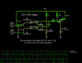
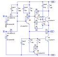
i would use for 12V https://en.wikipedia.org/wiki/High_Threshold_Logic
or HIGH_NOISE_IMMUNITY_LOGIC.jpg (now Spice verified) with minor change HiL - Test - x-a-1.png
 
Last edited:

Thread Starter

Ron Watkins

Joined Jun 5, 2018
47
You're using a circuit simulator. It should be straightforward have it tell you how it works. What do R2 and R4 do?
I can see that R2 and R4 create a voltage divider, which sets the emitter voltage to 6V instead of the normal GND. AFAIK that means that when Q1 is conducting, that we have 6V going to Q2, and when Q1 is open I don't see any voltatage going into Q2. So, that implies that Q2 is either 6V or floating, and I think that means it should always be conducting, but it's not. So im still lost as to how this works.
 

dl324

Joined Mar 30, 2015
18,445
So im still lost as to how this works.
In your original circuit, the emitter of the transistor was grounded. That meant the transistor was on when the base voltage increased to about 0.7V.

By having a voltage divider on the emitter that set the voltage to 6V, the transistor turn on voltage increases by 6V.
 

crutschow

Joined Mar 14, 2008
38,629
So, that implies that Q2 is either 6V or floating
Q2's what is either 6V or floating?
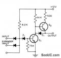
When Q1 is off there it has no collector current, so Q2 has no base current and is also off, and its output is at ground.
When Q1 turns on it conducts, so there is now also current flowing through Q2's base-emitter junction, and it turns on in a saturated state, so its output goes to very near 12V.
Remember that the normal current flow in a PNP is from emitter to base, and emitter to collector, thus the base of Q2 only has to be about 0.7V below 12V (11.3V) for it to turn on.
So both Q1 and Q2 turn on and off together.
 

Thread Starter

Ron Watkins

Joined Jun 5, 2018
47
This is all really great info. Ill do some more work on my side to see if I can come up with a simplified circuit which acts as a simple inverter (which all my diagrams to-date have been targeting).
I also liked the DTL design someone posted earlier, although I haven't had any chance to play with that in ltspice very much.
Im anxious to actually get some parts on a breadboard and see how it works.
If I can get some simple gate desing then I want to cr
can be easily converted more usable OR gate (!click to Falstad) ...
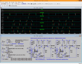
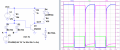
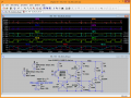
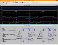
View attachment 183066 fast(=relatively carelessly) optimized for fast transition speeds & short delays , (converted to NOR to be able to use it as a base for other logic functions) → quick eval. of that type → View attachment 183083
Do you have the file from ltspice saved somewhere I can grab it? It's difficult to make out the details.
 

Bordodynov

Joined May 20, 2015
3,431
Here's the schematic. Due to the use of two transistors it was possible to obtain a low input current and a high (up to 500 mA) output current. I.e. the given valve has the big factor of branching ~2500 (if speed is not necessary).
 

Attachments

dl324

Joined Mar 30, 2015
18,445
Ill do some more work on my side to see if I can come up with a simplified circuit which acts as a simple inverter (which all my diagrams to-date have been targeting).
I also liked the DTL design someone posted earlier, although I haven't had any chance to play with that in ltspice very much.
A DTL NAND gate with one input is an inverter.
 

ci139

Joined Jul 11, 2016
2,018
i won't upload the NOR test because without a lot of improvements (that are required) the real thing likely will never work (because the spice is more optimistic , coherent and stable than the real life circuit) there would be a point trying the pre-previous NAND however ?
 

Attachments

ci139

Joined Jul 11, 2016
2,018
??? BAT54.pdf ((just confirming coz shcottkies have large junction capacities))
. . .
Reverse Leakage Current (Note 7)IR 2.0μA (@ VR= 25V)
Total Capacitance CT 10pF (@ VR= 1.0V, f = 1.0MHz)
Reverse Recovery Time tRR 5.0ns (@ IF= 10mA through IR= 10mA to IR= 1.0mA, RL= 100Ω)

. . .
looks ok !! but they (schottky diodes) still may cause "fancy responce" !!
 

Thread Starter

Ron Watkins

Joined Jun 5, 2018
47
Probably not, I was interested in the CMOS only due to it's greater voltage range, my project needs to use 12V instead of 5V, so I thought I could use CMOS as a way to take the TTL type of representation and get it to work at 12V.
 

ci139

Joined Jul 11, 2016
2,018
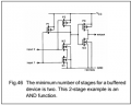
more confusing options :: vvr-NAND.png

——————————————
How do you like the 74LS
not really coz
how it's actually implemented
some funny things in related subjects ↑↑ (&youtube)
Probably not, I was interested in the CMOS only due to it's greater voltage range, my project needs to use 12V instead of 5V, so I thought I could use CMOS as a way to take the TTL type of representation and get it to work at 12V.
"Less is more" . . . carry out your initial idea - don't float too far from it (if it's just to blink a led attached to NOT gate -- it'll be good -- you're not braking a Guinness record here -- just a presentation)
 

Attachments

Last edited:
Top