Help with design of BJT logic gates

Thread Starter

Ron Watkins

Joined Jun 5, 2018
47
Thanks to everyone, I think I have enough info to try and build a physical circuit on a breadboard at this point without having all the parts explode on me.
I used the 470ohm resistor because I wanted to make sure the LED turned on, and I need at least 20ma to do that, so by using the 470 I would make sure to have enough for it to light. If I went to a 560 or higher resistor then the LED wouldn't get the 20ma needed to light.
I also like the comment about only driving a LED using the buffer circuit. Initially I was thinking about having all the gates be able to drive an LED, but in practice that wouldn't be normal, the gates output would only need enough current to drive other gate inputs, so that makes sense.
 

dl324

Joined Mar 30, 2015
18,445
Im just not clear on the diode configuration for the DTL
What isn't clear?

The thing I like about DTL is that a single transistor can be used for a NAND gate with 2-8 (or more) inputs. You just keep adding diodes. Since discrete diodes cost a penny and transistors cost a nickel or dime, it reduces cost. It also reduces wiring area and complexity.

If you're going to make "boards" for gates, NAND allows you to synthesize any logic combination.
 

dl324

Joined Mar 30, 2015
18,445
I used the 470ohm resistor because I wanted to make sure the LED turned on, and I need at least 20ma to do that, so by using the 470 I would make sure to have enough for it to light. If I went to a 560 or higher resistor then the LED wouldn't get the 20ma needed to light.
Check the datasheet again. 20mA is probably the maximum continuous forward current. You can operate at lower currents. You won't be able to tell the difference in brightness with 19.3mA vs. 20mA.
 

crutschow

Joined Mar 14, 2008
38,625
As for clean switching, it was my thought that the transistor would go directly from cut-off to saturation without passing through an amplification region. Is it possible to do this? If not, and I have to go through the amplification region, then I wanted it to be as small as possible to avoid undefined logic states as can be seen in the graphs I showed earlier.
Did you read what I said in my previous post about signal rise time?
You need to more carefully read the answers to your questions.

The transistor always goes through the active region when switching so you use a fast input signal rise and fall time to minimize the time in the active region.
Your simulations used a very slow (1 second) rise time.
Use a microsecond or less.
 

Alec_t

Joined Sep 17, 2013
15,146
I wanted to make sure the LED turned on, and I need at least 20ma to do that
You almost certainly don't. The datasheets of many LEDs specify a maximum 20mA, but it's bad practice to use components at their maximum rating. A modern LED will be adequately bright at just a few mA.
 

Thread Starter

Ron Watkins

Joined Jun 5, 2018
47
Check the datasheet again. 20mA is probably the maximum continuous forward current. You can operate at lower currents. You won't be able to tell the difference in brightness with 19.3mA vs. 20mA.
Oops, my bad, I thought that was the minimum. I just saw other circuits where they use a 470 with LED, so thought that was the better choice.
 

MrAl

Joined Jun 17, 2014
13,751
Hi,

You should not start with a logic gate. You should start with a single transistor and two resistors Rc collector and Rb base.
Drive the Rb base resistor with a pulse source and see how the collector voltage goes up and down.
Make the Rb base resistor about 10 times the value of the Rc collector resistor unless you need more speed.
Thus if Rc is 100 Ohms then make Rb 1000 Ohms.
Run that a few times and see what happens at the collector.
This will give you insight as to what you need in a logic gate too.

When designing the gates, try to keep the output low level down to maybe 0.5v and that means just one transistor. If you use two in series you get an output voltage that may be a little too high.
Note that if you put two transistors in parallel (except for the bases) you can make any gate.
The first type you get is a NOR gate because if either base is driven high the output goes low.
Now if you use two more transistors on the inputs you get an AND gate because you have to drive both input transistor bases high in order to get a high output.
Alternately, one transistor makes a negative logic NAND gate because both inputs driven low produces a high output.

There are other ways to do this too and if you want a totem pole output you need to add a few more components.
 

Thread Starter

Ron Watkins

Joined Jun 5, 2018
47
It's my plan to just do a single converter/inverter gate first, as you say with a single transistor.
Im not familiar with the "speed" issue you mention between the ratio of Rc to Rb. Can you elaborate on that?
Ill probably try to start with a 680 for Rc and a 6.8k for Rb and see what the currents and voltages look like.
I will want to light up an LED and use a push-button switch to drive the input.
This will just be to get a feel for how it works, and from there I can try to add more transistors (or diodes as recommended).
It will take me a few days (probably the weekend) before I get all the parts together.
 

dl324

Joined Mar 30, 2015
18,445
It's my plan to just do a single converter/inverter gate first, as you say with a single transistor.
If you aren't set on using RTL, I'd recommend going with DTL. A NAND with 1 input is an inverter. I've already gone through the design process for DTL at 5V using BC547. Using that as an example, you should be able to do choose appropriate resistors for 12V and 2N2222.
 

MrAl

Joined Jun 17, 2014
13,751
It's my plan to just do a single converter/inverter gate first, as you say with a single transistor.
Im not familiar with the "speed" issue you mention between the ratio of Rc to Rb. Can you elaborate on that?
Ill probably try to start with a 680 for Rc and a 6.8k for Rb and see what the currents and voltages look like.
I will want to light up an LED and use a push-button switch to drive the input.
This will just be to get a feel for how it works, and from there I can try to add more transistors (or diodes as recommended).
It will take me a few days (probably the weekend) before I get all the parts together.
Hello again,

The speed issue is related mostly to the base resistor value. The higher the value, the slower the turn on and turn off speed. It is caused by the capacitance of the transistor combined with the base resistor value which gives us a time constant R*C. There is also a base charge issue that could result in very slow reaction time for the transistor.

We could talk about additional components that speed up the rise and fall times as well as the delay time. For a couple examples:
a Baker Clamp
a Snap Off circuit
a Reverse Bias circuit

but as you know you should just get the single transistor inverter working and study that first. That will help you a lot.
 

Thread Starter

Ron Watkins

Joined Jun 5, 2018
47
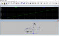
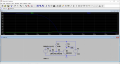
Followup question... Im modeling with LTSpice the following layout, mainly to get a feel for how the transistor would switch on/off. Im ignoring the active region and looking at the cut-off (far left) and saturation (far right) regions in the graph, and that is looking good. 0V input = 12V output, and visa-versa. Perfect. However, I noticed that the transistor switches around 0.7v input, and im wondering how I can shift that to be approx 6v input. The reason is that I want voltages < 6v to be considered low and >6v to be considered high. What im looking for is to shift the transition point from 0.7v to 6v.
upload_2019-8-1_8-53-51.png
 

Thread Starter

Ron Watkins

Joined Jun 5, 2018
47
That isn't the way logic gates are designed. If you were somehow able to make the switching voltage 6V, you wouldn't have any noise margin.
My concern is that we have the following ranges:
0v - 0.69v = cut-off
0.7v - 12v = saturation

So, I don't really have any headroom in the cut-off region, if my input is only slightly off, it could go above 0.7v and thus turn the transistor on. I wanted the transition to occur near the middle of the voltage range to allow for more input "slop" on both sides of the active region. Im worried that my input may go above 0.69v but still should be considered as a low input. Moving the switching point to 6v would be ideal, but just getting a bit more range on the low input would be helpful.
 

dl324

Joined Mar 30, 2015
18,445
Im worried that my input may go above 0.69v but still should be considered as a low input.
That's the purpose of the D3 in this circuit:

Which you've omitted in yours. Without D3, the circuit is marginal.
Moving the switching point to 6v would be ideal, but just getting a bit more range on the low input would be helpful.
That isn't an ideal design. Look at the TTL specs for LOW and HIGH input voltages.

For CMOS, they design the voltage for LOW to be up to 0.3Vdd and HIGH to be >= 0.6Vdd.
 

Thread Starter

Ron Watkins

Joined Jun 5, 2018
47
That's the purpose of the D3 in this circuit:

Which you've omitted in yours. Without D3, the circuit is marginal.
That isn't an ideal design. Look at the TTL specs for LOW and HIGH input voltages.

For CMOS, they design the voltage for LOW to be up to 0.3Vdd and HIGH to be >= 0.6Vdd.
What part number diode should be used?
 
Top