Feedback between multivibrator and opamp integrator?

RichardO

Joined May 4, 2013
2,270
From experimenting I didn't see much voltage gain for the triangle when lowering R1. I think the typical sink current for the LM393 is 16mA but I can't find it in the datasheet right now. This may be one reason crutschow has a 2k pull-up resistor.
I checked and you are right the _typical_ sink current is 16ma minimum. But...it can be as low as 6ma depending on temperature and he luck of the draw for the device you actually have.

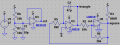
The way to choose the values of R1, R2 and R3 resistor value is to trade off the high state output voltage when loaded by the feedback resistor against the saturation voltage when in the low state. You want to use most of the maximum allowed sink current when the drop across R1 is about equal to the saturation voltage. You don't want to use all of the sink current in the pullup resistor or there will not be any current to drive stray capacitances.

But apart from these things, the reason for lowering this value is perhaps to reduce the time constant associated with stray capacitance of the breadboard
Correct. :) 
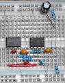
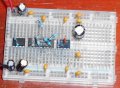
There is also coupling between contact strips -- but that is another issue.

I'm not too concerned with low supply voltages right now, for one because it allows me to properly drive most opamps that I have. The 16V comes from two dying 9V batteries. I came across the LM318 which has a very high slew rate, might be a good part.
The 16 volts is a good idea. I started my learning about the limitations of the SBB (Solderless BreadBoard) using the LM318. A nice part for its time but it tends to oscillate if you don't do proper layout of the wiring, component placement and power supply bypass. Once you make a LM318 behave you are a long way to understanding what will and what not will work at high frequencies.

Yes, I see how the hysteresis thresholds set the triangle amplitude given a fast enough comparator. Going by your instructions I lowered the resistor values of the hysteresis ratio. This had great effect on the triangle amplitude though I don understand why.
The comparator switches when the voltage at its positive input equals the voltage at its negative input. this voltage is set by the output voltage of the comparator and the ratio of R1 to R2. Keep in mind that the current is the same through both R1 and R2. Why? Because they are in series and the input of the comparator is high impedance and, therefore, draws little current away from R1 and R2.

For example, if R2 is 10 times the value of R1 the comparator will switch at about 2.25 volts and 2.75 volts because there is about 0.25 volts across R1 when the comparator switches.
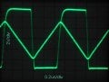
Anyway, I get 600kHz now and the waveform isn't too bad. After de-sloppifying the breadboard the squarewaveform improved, but the triangle still has a slight nick at the tops. EDIT: The 47pF speed-up capacitor across R1 is missing from the diagram.
Great.
A slow risetime of the squarewave will cause rounding of the peaks of the triangle wave.

Overshoot on the square wave will cause "peaking" on the tips of the triangle wave. Do you really have overshoot as shown in your waveforms? You do have your scope probe properly compensated don't you? ;)

You can also get a glitch at the peak of the triangle if some of the square wave couples directly into the input of the integrator. This is the likely cause. Check your layout on the SBB.

One final source of a glitch is resistance in series with the timing capacitor. I doubt this is your problem.

Glitches show up better (better? :rolleyes:) with faster op-amps.

EDIT2: P.s. Thanks for your 10MHz circuit! It is way beyond me but I'll study it and see if I can make sense of parts of it.
There are a lot of subtleties in that design. Feel free to ask as many questions as you want until you understand it all. :D
 

RichardO

Joined May 4, 2013
2,270
I thought of one other possibility for the nick in your triangle waveform. It might be caused by power sagging. This would be cured by a better bypassing, especially a larger bulk capacitor.
 

Thread Starter

hrs

Joined Jun 13, 2014
532
Overshoot on the square wave will cause "peaking" on the tips of the triangle wave. Do you really have overshoot as shown in your waveforms? You do have your scope probe properly compensated don't you? ;)
My probes look properly compensated, though 1X loads down the leading edge of the square wave significantly. 10X seems fine. It appears there really is overshoot.
You can also get a glitch at the peak of the triangle if some of the square wave couples directly into the input of the integrator. This is the likely cause. Check your layout on the SBB.
The glitches at the peaks coincide exactly with with the transition on the inverting input of the integrator. After adding 470uF + 100nF across the batteries and another 100nF across ground and the reference voltage, the glitch remains unchanged. The slew rate of the triangle is around the typical value of the TL072, maybe this is just pushing it too far for these parts? Oh, One thing I need to try is lower R1 and R2 further, 5k and 10k or so. EDIT: 4.7k/10k increases square wave peaking overshoot, 20k/39k almost eliminates any peaking overshoot, though the glitch seems unrelated.

I'll order some faster parts in a minute and see what a faster comparator does when it arives.
 

Attachments

Last edited:

Thread Starter

hrs

Joined Jun 13, 2014
532
Here's a small update for those interested.

First I swapped the LM393 for an LM319. The LM319 can handle 25mA of sink current. Reducing the pull-up resistor to 820 Ohms got rid of most of the square wave overshoot.

At some point I noticed a significant ripple/waveform of 1 or 2 volts p-p across the inputs of the TL072. This is far from the ideal op-amp. After swapping the TL072 for an LM318 the triangle amplitude reduced by half so I guess the propagation delay of the TL072 was getting significant. There's very little ripple across the inputs of the LM318.

Now there's still a slight glitch at the bottom of the triangle rising edge. I think this is due to the slight ringing at the bottom of the square wave falling edge. There's some rounding of the triangle peaks because the square wave edges are not fast enough. I bought some NE521s too which may clean up both waveforms. But first I'll play around with this circuit some more and see if I can get rid of the ringing.
 

Attachments

RichardO

Joined May 4, 2013
2,270
Here's a small update for those interested.

First I swapped the LM393 for an LM319. The LM319 can handle 25mA of sink current. Reducing the pull-up resistor to 820 Ohms got rid of most of the square wave overshoot.

At some point I noticed a significant ripple/waveform of 1 or 2 volts p-p across the inputs of the TL072. This is far from the ideal op-amp. After swapping the TL072 for an LM318 the triangle amplitude reduced by half so I guess the propagation delay of the TL072 was getting significant. There's very little ripple across the inputs of the LM318.

Now there's still a slight glitch at the bottom of the triangle rising edge. I think this is due to the slight ringing at the bottom of the square wave falling edge. There's some rounding of the triangle peaks because the square wave edges are not fast enough. I bought some NE521s too which may clean up both waveforms. But first I'll play around with this circuit some more and see if I can get rid of the ringing.
Nice.

That is not too much ringing. If your circuit is on a solderless breadboard then you will have a hard time reducing it. Better power supply bypassing may help. Add a 0.1uF ceramic caps from the ref signal to ground right at the LM318 _and_ the LM319, for instance.

I would really like to see a picture of your circuit. The fact your signals look so good I expect it to be quite pretty. :D:D
 

Thread Starter

hrs

Joined Jun 13, 2014
532
Add a 0.1uF ceramic caps from the ref signal to ground right at the LM318 _and_ the LM319, for instance.
Great, I'll give that a shot tomorrow.
I would really like to see a picture of your circuit. The fact your signals look so good I expect it to be quite pretty. :D:D
I'll make a picture tomorrow, though it's not very pretty at the moment. Those LM318 and LM319 are a cow to wire given that the output is on the other side of the DIP than the inputs. But I did go bananas with decoupling. I'll explain what I tried to do using the picture that I'll make.
 

RichardO

Joined May 4, 2013
2,270
Great, I'll give that a shot tomorrow.

I'll make a picture tomorrow, though it's not very pretty at the moment. Those LM318 and LM319 are a cow to wire given that the output is on the other side of the DIP than the inputs. But I did go bananas with decoupling. I'll explain what I tried to do using the picture that I'll make.
I look forward to your picture and explanation. A solderless breadboard is always a compromise between ease of wiring and high frequency performance.

The outputs being on the opposite side of the inputs. This reduces unwanted coupling from the output to input that can cause reduction of bandwidth or even oscillation.
 

Thread Starter

hrs

Joined Jun 13, 2014
532
These bead-like 100nF ceramic capacitors are impossible to wire directly across both power pins of a DIP so usually I place the cap directly at Vcc of the chip and snake the other leg of the cap to ground at the other side of the board. Then I thought this is probably pretty bad.

In the attached picture you can Vcc and GND going around in a horse shoe kind of shape with a bunch of 100nF/330nF ceramics, 10uF/47uF electrolytics and a 1u tantalum cap across Vcc and GND. The idea is then that I can decouple the Vcc pins to GND close by and decouple GND to Vcc close by. Whether this actually works I don't know. One thing to try might be to remove decoupling caps until it breaks down.
 

Attachments

RichardO

Joined May 4, 2013
2,270
These bead-like 100nF ceramic capacitors are impossible to wire directly across both power pins of a DIP so usually I place the cap directly at Vcc of the chip and snake the other leg of the cap to ground at the other side of the board. Then I thought this is probably pretty bad.

In the attached picture you can Vcc and GND going around in a horse shoe kind of shape with a bunch of 100nF/330nF ceramics, 10uF/47uF electrolytics and a 1u tantalum cap across Vcc and GND. The idea is then that I can decouple the Vcc pins to GND close by and decouple GND to Vcc close by. Whether this actually works I don't know. One thing to try might be to remove decoupling caps until it breaks down.
I really like the way you built the circuit. It has short leads and direct connections. :D:D The clean waveforms confirm the quality of your work. :)

Why do you have 2 buses assigned for each of the +5 volts and ground? It is obviously not causing a problem with your circuit but it might in more complex designs. This will happen when you need -5 volts for the NE521 comparator. Right now, having +/- 15 volts powering the LM318 and LM319 would probably give a bit better high frequency performance but would need more power buses as well.

I don't see the glitch that you mention is on the triangle. I suspect it is small enough that it is hidden by the square wave.

One possible source of a glitch in the triangle wave is some of the square wave coupling across the integrator resistor. This can be caused by the capacitance of the vertical contact strips of the SBB (solderless breadboard). This coupling can be reduced by grounding one of these contact strips. This acts as a shield shunting the coupled signal to ground instead of it getting into the input of the op-amp. (This coupling is not happening in your present wiring -- I mention it for future reference).

Could you post your schematic of what is on the breadboard? You caught me off guard with what appears to be a voltage reference chip.


Here are some of my philosophies, opinions and preferences. They are _not_ chiseled in stone... ;)
------------------------------------------------------------------------------------------------
-- Schematics are drawn with the inputs on the left and the outputs on the right.
-- They are also drawn with the most positive power supply voltage at the top and the most negative voltage at the bottom.

-- Power is brought in at the right, output side. Bulk (tantalum and electrolylic caps) bypassing is done where the power is brought into the breadboard.
-- I usually assign the power buses, from top to bottom, as +15, +5, ground and -5 or -15 on the bottom bus. This last one is a problem because there are usually only four power buses -- two at the top and two at the bottom. :(

-- This is such a problem that when I made my own PCB, soldered version of the SBB I put three power buses at both the top and bottom. :)
-- Some solderless breadboards are modular. This allows the use of two power buses at the top and two pairs of power buses at the bottom.

-- I build the circuit the same way. This makes the circuit easier to build and more likely to work the first time. It also makes it easier to troubleshoot if it doesn't work.
-- Having the circuit like this has another advantage. It reduces ground loops caused by current from the outputs being drawn through the input ground.

-- What about your circuit? It has inputs to both the op-amp and the comparator and outputs from both of them as well.
-- I always consider analog signals to be inputs and digital signals as outputs. This means that I would put the op-amp on the left and the comparator on the right.
 

Thread Starter

hrs

Joined Jun 13, 2014
532
Hi Richard and thank you for your continued interest :)
Why do you have 2 buses assigned for each of the +5 volts and ground? It is obviously not causing a problem with your circuit but it might in more complex designs. This will happen when you need -5 volts for the NE521 comparator.
I've added an annotated picture of the breadboard. The dark blue and red line are ground and Vcc respectively. The pink "circles" mark a total of 9 capacitors across Vcc and ground. The hope was to create a stable power voltage along the entire length of this power bus. With this in place I decoupled the Vcc pins to the ground bus at the top of the picture and the ground pins to the Vcc bus at the bottom of the picture. These pin decoupling capacitors are marked with blue "circles". This fancy-pants strategy proved unneeded because I just tested pulling out _all_ capacitors one at a time. All that is needed to prevent oscillation is a single 47uF electrolytic anywhere across the bus.

Right now, having +/- 15 volts powering the LM318 and LM319 would probably give a bit better high frequency performance but would need more power buses as well.
I was trying to tread softly here because LM319 can only tolerate a differential input voltage of 5V and I think it's 1V for the LM318. But I will try to up the voltage keeping an eye on the differential input voltages. Unfortunately I don't have a variable power supply, that should be my next project ...
I don't see the glitch that you mention is on the triangle. I suspect it is small enough that it is hidden by the square wave.
It's like the nick that was there before, but less pronounced and on the other side of the slope.

One possible source of a glitch in the triangle wave is some of the square wave coupling across the integrator resistor. This can be caused by the capacitance of the vertical contact strips of the SBB (solderless breadboard). This coupling can be reduced by grounding one of these contact strips. This acts as a shield shunting the coupled signal to ground instead of it getting into the input of the op-amp. (This coupling is not happening in your present wiring -- I mention it for future reference).
Excellent, thank you. I will keep this in mind.
Could you post your schematic of what is on the breadboard? You caught me off guard with what appears to be a voltage reference chip.
It is the schematic from post #25 but I've included it again. It shows none of the decoupling caps except the one across the voltage divider for the reference voltage. [Edit]You talked a bit about lowering resistor values in order to drive stray capacitance better, therefore I decided to introduce a voltage follower for the ref voltage. This is perhaps a major contributor to the stability of the circuit.[/Edit]

Here are some of my philosophies, opinions and preferences. They are _not_ chiseled in stone... ;)
------------------------------------------------------------------------------------------------
-- Schematics are drawn with the inputs on the left and the outputs on the right.
-- They are also drawn with the most positive power supply voltage at the top and the most negative voltage at the bottom.

-- Power is brought in at the right, output side. Bulk (tantalum and electrolylic caps) bypassing is done where the power is brought into the breadboard.
-- I usually assign the power buses, from top to bottom, as +15, +5, ground and -5 or -15 on the bottom bus. This last one is a problem because there are usually only four power buses -- two at the top and two at the bottom. :(

-- This is such a problem that when I made my own PCB, soldered version of the SBB I put three power buses at both the top and bottom. :)
-- Some solderless breadboards are modular. This allows the use of two power buses at the top and two pairs of power buses at the bottom.

-- I build the circuit the same way. This makes the circuit easier to build and more likely to work the first time. It also makes it easier to troubleshoot if it doesn't work.
-- Having the circuit like this has another advantage. It reduces ground loops caused by current from the outputs being drawn through the input ground.

-- What about your circuit? It has inputs to both the op-amp and the comparator and outputs from both of them as well.
-- I always consider analog signals to be inputs and digital signals as outputs. This means that I would put the op-amp on the left and the comparator on the right.
Thanks, this is all great stuff. I try to use common sense but the analog input / digital output would never had occurred to me. Such conventions will probably be helpful in large, complex circuits.

I have one more inane noob question if you don't mind. I noticed that when I clamp a 470 Ohm resistor to the tip of my scope probe and stick the other end of the resistor in the square wave output there is zero ringing, it's perfect. But what happens here?
- The ringing is still there but we are now blind to it.
- The scope probe introduces the ringing and the resistor does ... something.
- We can never know because the measurement alters the circuit.
- Other ...
 

Attachments

Last edited:

RichardO

Joined May 4, 2013
2,270
I've added an annotated picture of the breadboard. The dark blue and red line are ground and Vcc respectively. The pink "circles" mark a total of 9 capacitors across Vcc and ground. The hope was to create a stable power voltage along the entire length of this power bus. With this in place I decoupled the Vcc pins to the ground bus at the top of the picture and the ground pins to the Vcc bus at the bottom of the picture. These pin decoupling capacitors are marked with blue "circles". This fancy-pants strategy proved unneeded because I just tested pulling out _all_ capacitors one at a time. All that is needed to prevent oscillation is a single 47uF electrolytic anywhere across the bus.
Got it. Now the "extra" bus connections make sense. With all the bypassing the double buses probably do help a bit. The reason I say "probably" is that you have added the inductance from the top to the bottom of the SBB to the power supply impedance for the added buses -- this is because of the long connection.

Good experiment. Keep in mind that oscillation is not your only consideration. You are also trying to keep the power low impedance for fast changes in the current being drawn by the circuit. For instance, if the impedance gets too high then there output of the comparator output will not have enough current for a fast transition. This current is needed to drive the load and stray capacitances.

I was trying to tread softly here because LM319 can only tolerate a differential input voltage of 5V and I think it's 1V for the LM318. But I will try to up the voltage keeping an eye on the differential input voltages. Unfortunately I don't have a variable power supply, that should be my next project ...
No problem for the LM318. I has diode clamped inputs and can tolerate input voltages equal to the power supply voltages. Keep in mind, though, that because of the diode clamping, the input current is limited to an absolute maximum of 10 ma caused by voltage _between_ the inputs. (These input clamp diodes can create havoc in peak detector circuits. Ask me how I know :rolleyes:).

The comparator input is another matter. Again, the inputs can tolerate voltages equal to the power supply voltages. However, If more than 5 volts is applied between the inputs then the base to emitter junctions will break d own (Zener). This will not cause a failure of the part if current is limited to a few milliamps. But, the breakdown will cause the input transistors to become noisy.

For fun, take a look at the equivalent circuit diagrams in the LMN318 and LM319 data sheets. There is a lot to be learned doing that. For instance, the input clamp circuit is shown in the LM318 schematic. The LM319 schematic shows no input clamping.

It's like the nick that was there before, but less pronounced and on the other side of the slope.
I must be blind because I just don't see it. It is obvious that you have a good handle on the problem since is is so greatly reduced. :D


It is the schematic from post #25 but I've included it again. It shows none of the decoupling caps except the one across the voltage divider for the reference voltage. [Edit]You talked a bit about lowering resistor values in order to drive stray capacitance better, therefore I decided to introduce a voltage follower for the ref voltage. This is perhaps a major contributor to the stability of the circuit.[/Edit]
I am sure the buffer helped at low frequencies. It does not help at frequencies over a few hundred kiloHertz. This is because the op-amp has a gain-bandwidth product of only 10 MHz. this means the op-amp only has an open loop gain of 1 at 10 MHz. :( Your square wave has a falltime of about 50ns. This is equivalent to about 7 MHz. There is no way the op-amp can keep a stable output if that pulse is applied to its output because of a changing load caused by the square wave transitioning.

The fix is to put bypass caps on "Ref" at the inputs of the LM319 and LM318. Be warned that some (actually many) op-amps an oscillate if you put too large a capacitance on the output. You are probably OK using 0.1 uF caps in your circuit.

Thanks, this is all great stuff. I try to use common sense but the analog input / digital output would never had occurred to me. Such conventions will probably be helpful in large, complex circuits.
"Common sense" is often learned and not so common. Glad I could help.

I have one more inane noob question if you don't mind. I noticed that when I clamp a 470 Ohm resistor to the tip of my scope probe and stick the other end of the resistor in the square wave output there is zero ringing, it's perfect. But what happens here?
- The ringing is still there but we are now blind to it.
- The scope probe introduces the ringing and the resistor does ... something.
- We can never know because the measurement alters the circuit.
- Other ...
All of the above. ;)
The probe can induce ringing for two reasons.
The first is that the probe introduces added capacitance loading on the signal. In an op-amp, this cause phase shift reducing the stability of the circuit. The output of the LM319 does not have feed back so this is not the problem.

The second is that the probe is adding inductance into the measurement. This is mostly caused by the ground lead of the probe. When the probe sees a fast changing signal some of the signal is dropped across the inductance of the ground lead. This inductance combined with stray capacitance can cause a resonance and, therefore, ringing. This is probably what you are seeing.

When you connect the 470 ohm resistor you are doing two things. The resistor reduces the Q of the resonant circuit damping the ringing. It also isolates the circuit from the probe's capacitance. I think the reduction in the Q is what gets rid of your ringing. Note that the resistor is also reducing the bandwidth of the oscilloscope measurement because the resistor in combination with the probe capacitance is a low pass filter. This will make the scope somewhat blind to very high frequency ringing.

Yes the measurement _is_ effecting the measurement. See my tagline. :D

Always remember: Your measuring instrument is part of the circuit you are measuring.
-- Bob Sides, Tech school instructor
 

Attachments

Thread Starter

hrs

Joined Jun 13, 2014
532
(These input clamp diodes can create havoc in peak detector circuits. Ask me how I know :rolleyes:).
How do you know? :D
The fix is to put bypass caps on "Ref" at the inputs of the LM319 and LM318. Be warned that some (actually many) op-amps an oscillate if you put too large a capacitance on the output. You are probably OK using 0.1 uF caps in your circuit.
Looks like it oscillates! Adding a 100nF cap at the ref pins increased the ripple by an order of magnitude. With a converted PC power supply I can get +/- 12V and use ground for the ref voltage while making sure not to make the scope ground common with Vcc _again_. Did you know that the fusing current of an alligator clip lead is right around the over-current trip point of a PC power supply?

At 1.3 MHz using +/- 12V the edges are about 100ns or 1/4 of half a period. The triangle amplitude is quite sensitive again to the frequency so I think it's time to try the NE521. I'll bump this thread one more time then I get around to doing that.

Cheers.
 
Last edited:

RichardO

Joined May 4, 2013
2,270
How do you know? :D
Drat, I was hoping you wouldn't ask. ;) Now I have to remember the details...
I think it was a circuit in a light pen. The light pen gave an output pulse to indicate where it was pointing on the face of a CRT. A comparator detected the peak of the bright spot as it passed the pen. What was happening is that a cap stored the peak voltage for the spot and that voltage was compared to previous voltages. If the new peak voltage was greater then a pulse was generated. The problem was that the diodes between the comparator inputs would connect the capacitor too the input voltage and discharge it.

I will try to track down a schematic of the peak detector so this makes more sense.

Looks like it oscillates! Adding a 100nF cap at the ref pins increased the ripple by an order of magnitude.
I am a bit surprised. I thought those op-amps were pretty stable. Wait. I am thinking of the TL-082. I have never used the NE5532.

One fix is to add a small resistor (50 to 100 ohms) between the op-output and the caps. Since you are not drawing any current from the reference this shuld not create any unexpected errors.

With a converted PC power supply I can get +/- 12V and use ground for the ref voltage while making sure not to make the scope ground common with Vcc _again_. Did you know that the fusing current of an alligator clip lead is right around the over-current trip point of a PC power supply?
I do now. :eek:

At 1.3 MHz using +/- 12V the edges are about 100ns or 1/4 of half a period. The triangle amplitude is quite sensitive again to the frequency so I think it's time to try the NE521. I'll bump this thread one more time then I get around to doing that.
The edges of the LM319? Are you still using 5 volts for the output power supply? If not, you may want to. A 12 volt voltage change may take longer than a 5 volt change.
 

Thread Starter

hrs

Joined Jun 13, 2014
532
I will try to track down a schematic of the peak detector so this makes more sense.
That would be interesting but only if it's not too much trouble.
The edges of the LM319? Are you still using 5 volts for the output power supply? If not, you may want to. A 12 volt voltage change may take longer than a 5 volt change.
Yes, the edges of the LM319 making a transition from -12V to +12V. I think you mean the pull-up voltage. The GND pin on the LM319 apparently limits the low voltage output. With GND on -5V and the pull-up resistor on +5V the waveform looks much better.
 

RichardO

Joined May 4, 2013
2,270
That would be interesting but only if it's not too much trouble.

Yes, the edges of the LM319 making a transition from -12V to +12V. I think you mean the pull-up voltage. The GND pin on the LM319 apparently limits the low voltage output. With GND on -5V and the pull-up resistor on +5V the waveform looks much better.
I think there is a version of the peak detector in the National Semiconductor Linear Applications Manual. I will look there first to see if it makes any brain cells twitch. :D

Good to hear that the lower voltage swing is faster. Don't forget that the NE521 only runs on plus and minus 5 volts. This may be a step back from what you are doing here. It may force you to do some kind of switched current source instead of integrating a voltage.


In case you have never looked at how the ICL8038 function generator chip works, I have attached the data sheet and some application notes. Note that the 8038 does not use an integrator but instead it uses current sources to charge and discharge the timing cap.
 

Attachments

Thread Starter

hrs

Joined Jun 13, 2014
532
Good to hear that the lower voltage swing is faster. Don't forget that the NE521 only runs on plus and minus 5 volts. This may be a step back from what you are doing here. It may force you to do some kind of switched current source instead of integrating a voltage.
Is this because there isn't enough voltage and/or current to drive from the NE521 to the integrator or that the LM318 needs more supply voltage for sufficient output swing?
In case you have never looked at how the ICL8038 function generator chip works, I have attached the data sheet and some application notes. Note that the 8038 does not use an integrator but instead it uses current sources to charge and discharge the timing cap.
Thanks, I'll have a look and see if I can figure out the general idea. If I understood correctly you are doing a similar thing in the generator you are now developing.

A while ago I came across the attached schematic on the eevblog forum though I can't find the thread anymore. I think the gist was that you get good decoupling between frequency and amplitude adjustment and a high degree of symmetry of the waveform. Though I would think the flip-flop would need to have as fast or faster edges than the comparator. So an LM319 and a CD4013 might be a good match but an NE521 would be wasted on a CD4013.
 

Attachments

RichardO

Joined May 4, 2013
2,270
Is this because there isn't enough voltage and/or current to drive from the NE521 to the integrator or that the LM318 needs more supply voltage for sufficient output swing?
What I should have said is that the NE521 has a TTL output so it can only swing between ground and 5 volts. (Actually, more like 0.2 volts and 3.5 volts). It is nice thatthe LM319 can swing more or less centered around ground. This lets you center the triangle around ground.

And, since you mention it, the LM318 may not work very well on +/-5 volt power. It is an old part that was expected to be powered by +/-15 volts.

Thanks, I'll have a look and see if I can figure out the general idea. If I understood correctly you are doing a similar thing in the generator you are now developing.
The 8038 uses 2 current sources. On is a positive current (I) and the other is a negative current twice the positive current (-2I). When the negative current source is turned off, the timing cap charges at +1I. When the negative current source is turned on the timing cap is discharged at +I +(-2I) = -I of current.

Yes I am doing the same basic scheme. The main difference is I have -I and +2I with the +2I switched.

By the way there is another common way of doing this. That is to have 2 matched current sources -- +I and -I. When one is on the other is off and vice versa.

This is how it is done in old WaveTek and Tektronix function generators. As further abuse, here is a link to the Tek FG504 manual, a 40 MHz function generator:
http://bama.edebris.com/download/tek/fg504/FG504.pdf

A while ago I came across the attached schematic on the eevblog forum though I can't find the thread anymore. I think the gist was that you get good decoupling between frequency and amplitude adjustment and a high degree of symmetry of the waveform. Though I would think the flip-flop would need to have as fast or faster edges than the comparator. So an LM319 and a CD4013 might be a good match but an NE521 would be wasted on a CD4013.
That circuit is really slow. The LM311 is slower that your LM319 and the CD4013 is not much faster. The sum of the LM311 and CD4013 delays is going to approach a microsecond. I didn't bother looking up the speed of the op-amps...

Note that the NE521 has the gates to make a set/reset flip-flop built in. No need for the CD4013. If you wanted to do a version of this circuit using your LM319 you could use a 74HC00 for the flip-flop. The 74HC00 would give nice clean 0 and 5 volts for your integrator.
 

Thread Starter

hrs

Joined Jun 13, 2014
532
What I should have said is that the NE521 has a TTL output so it can only swing between ground and 5 volts. (Actually, more like 0.2 volts and 3.5 volts). It is nice thatthe LM319 can swing more or less centered around ground. This lets you center the triangle around ground.
Looking at the schematic of the NE521 you probably can't tie the GND pin to V- like you can on the LM319.

That circuit is really slow. The LM311 is slower that your LM319 and the CD4013 is not much faster. The sum of the LM311 and CD4013 delays is going to approach a microsecond. I didn't bother looking up the speed of the op-amps...
I was referring more to the topology, i.e. two comparators feeding a flip-flop. It seems to be used in a lot of places including the ICL8038. There isn't much on why this is used but here's what I found and some of my own assumptions:
- The thresholds are now applied externally and not a function of the circuit itself. This is said to make them more predictable. I guess I can see that.
- It makes the circuit independent of supply. I can see that this would work with a zener based threshold, but not with a voltage divider.
- It can be a means to control duty cycle by setting asymmetrical thresholds.
- Frequency and amplitude become more independent.
- A comparator is less likely to swing to the rails symmetrically than a flip-flop. This makes the positive and negative constants of integration provided by the flip-flop (very close to both rails) more predictable giving a more symmetrical triangle. This would work when feeding an integrator directly from the flip-flop.
Is that about correct?

Note that the NE521 has the gates to make a set/reset flip-flop built in. No need for the CD4013.
By using the strobes somehow? But that would still give the same TTL output. Which would be irrelevant if you are switching current sources so there must be another reason for the flip-flop.

I've downloaded the FG504 manual, reading it is on my to-do list. :D
 
Top