Feedback between multivibrator and opamp integrator?

RichardO

Joined May 4, 2013
2,270
Looking at the schematic of the NE521 you probably can't tie the GND pin to V- like you can on the LM319.
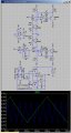
Correct. The output is from the NE521 can only be a TTL level because the internal gates must be powered from +5 volts and ground.

I was referring more to the topology, i.e. two comparators feeding a flip-flop. It seems to be used in a lot of places including the ICL8038. There isn't much on why this is used but here's what I found and some of my own assumptions:
1- The thresholds are now applied externally and not a function of the circuit itself. This is said to make them more predictable. I guess I can see that.
2- It makes the circuit independent of supply. I can see that this would work with a zener based threshold, but not with a voltage divider.
3- It can be a means to control duty cycle by setting asymmetrical thresholds.
4- Frequency and amplitude become more independent.
5- A comparator is less likely to swing to the rails symmetrically than a flip-flop. This makes the positive and negative constants of integration provided by the flip-flop (very close to both rails) more predictable giving a more symmetrical triangle. This would work when feeding an integrator directly from the flip-flop.
Is that about correct?
1- Yes, the thresholds can be made independent of the rest of the circuit.
2- Sort of. Now the thresholds can be as accurate as you want. They could be derived from the power supplies and voltage dividers if you are not too concerned about accuracy or stability. At the other extreme, they could be derived from precision voltage references which would be much more accurate and stable.
3- You could control symmetry this way. The disadvantage is that the amplitude of the triangle would also vary. The frequency would probably vary when you change the duty cycle which is normally undesirable.
4- I don't follow your thinking on this. It may or may not be true.
5- The problem with the comparator using hysteresis is that there are a lot of parts determining the triangle amplitude and therefore the frequency. The flip-flop may or may not be more precise in its output amplitude. A CMOS flip-flop will have a nice predictable output voltage if(!) it does not have to deliver any current to the integrator. A TTL flip-flop output amplitude will be not as good as a CMOS flip-flop no matter what.

By using the strobes somehow? But that would still give the same TTL output. Which would be irrelevant if you are switching current sources so there must be another reason for the flip-flop.
If you look at the block diagram of the NE521 you will see that is has two identical circuits. Each circuit has a strobe and a comparator driving a 2-input NAND gate. You can make a set/reset flip by connection each strobe to the opposite NAND gate input. When wired this way, the comparators are the set and reset signals of the flip-flop. The function of the flip-flop is to get the latching effect that is supplied by the hysteresis in the single-comparator circuit. Now, the comparators don't have to have the inaccurate hysteresis setting the thresholds.

I've downloaded the FG504 manual, reading it is on my to-do list. :D
You can read that when you are having a hard time getting to sleep. ;)
 

Thread Starter

hrs

Joined Jun 13, 2014
532
RichardO said:
Note that the NE521 has the gates to make a set/reset flip-flop built in.
Like in the WiggTak989! :D I'll be trying that once I can get current sources to work on a single comparator.

RichardO said:
hrs said:
[Reasons for the flip-flip]
4- Frequency and amplitude become more independent.
4- I don't follow your thinking on this. It may or may not be true.
5- The problem with the comparator using hysteresis is that there are a lot of parts determining the triangle amplitude and therefore the frequency.
It's one of the things I read somewhere. I thought the reason might be variation in loading between R2, R3 and R5 for varying values (schematic in post #31). Reason 5- sounds like a better one :). And I totally missed the dual comparator set-up lacks hysteresis/latching!

In new experiments I replaced the LM319 with an NE521. I didn't record the schematic but it's pretty much the same as previously with the unused comparator properly terminated. NE521 on +-5V, LM318 on +-12V. It won't go beyond ~3MHz. The attached photo is from a measurement using a make-shift probe tip ground, without it the was severe ringing. Do you think the distorted triangle wave tops are the LM318 trying to integrate the ringing or is it just oscillating at the fast edges?


After slowly getting nowhere with switched current sources I reached the current state per attached "switched current source.jpg". Obvious problems are triangle biasing and current spikes. And it just doesn't work. The diode bridge is the only switch that I could come up with that barely works.

In "WiggTak989 partial schematic.jpg" I've tried to guess some functional blocks.
How does the WiggTak989 accomplish switching? I especially don't understand how the comparator output can have any influence on the switch.
Are the caps on the source/sink there to form a LPF to suppress switching noise?
What is the purpose of the diodes in FB loop?
 

Attachments

RichardO

Joined May 4, 2013
2,270
I think the junk on the peaks of the triangle wave is probably the LM318 oscillating. As best I can tell there are about 3 cycles in about 40 ns. This would be about 60 MHz which might be possible with the LM318 -- I am not sure since it has been a while since I have seen an LM318 oscillate.

I'm not convinced your current sources work. As I see it, one problem with your current sources is that the LT1001 is does not have rail to rail inputs and outputs. The LT1001 won't operate properly closer than a couple of volts from either power supply. Look at the 2N3906, for example, it never turns off because the emitter can be at 12 volts but the LT1001 is only specified to get to something like 10 volts. Try an LT1630 in your simulation and see if it works better.

A way to test a current source is to use a resistor as a load to ground. The voltage across the load resistor should track Vin. It looks like the biasing is not right for the current sources. I would expect the current through the load resistor to be zero if the input voltage is zero.

As to the diode current steering switch... I don't have time to do the analysis right but I think the biasing for the current switch and Q3 are not right to center the output of the current switch at Vref (2.5 volts). Similarly, I think that the input to the hysteresis switch also has to be biased to put the thresholds centered around Vref (2.5 volts).

I recommend that you replace Q3 with an op-amp integrator. Drive the (inverting) input of the integrator directly from the junction of D2 and D4. Bias the non-inverting input of the integrator at Vref. If I am right, you should now get a clean triangle. If not, post your .asc file here and I will try it to see where I went wrong.


In the partial WiggTak diagram you don't quite have it right. The transistors are part of the current source. Only the diodes comprise the current steering switch.
 

RichardO

Joined May 4, 2013
2,270
@hrs:
Here is a simulation to let you play with the diode switch.

Note there is a glitch at the peak of the triangle. I suspect that the cause is either the square wave coupling into the timing cap through the diode switch or the reverse recovery time of the diodes. Fixing it is left as a challenge to the reader. ;)

upload_2018-4-12_10-34-31.png
 

Attachments

Thread Starter

hrs

Joined Jun 13, 2014
532
Thank you, Richard! I'll go over your pointers and play around with the diode switch as time permits.
 

RichardO

Joined May 4, 2013
2,270
Thank you, Richard! I'll go over your pointers and play around with the diode switch as time permits.
Hints...

The current steering diodes have several undesirable characteristics such as inductance, capacitance, leakage, forward drop, reverse recovery time. Here are some things to consider in your analysis:

What effect does the forward drop of the diodes have on the requirements of the square wave driving switch and the way the timing capacitor is charged?

Also, what constraints are put on the current sources by the forward drop, square wave voltages and timing cap voltages?

When does the capacitance of the diodes effect the circuit? What are ways to reduce the effect of the diode capacitances?

How severe is the leakage currents of the diodes? How can the leakage current effect be minimized?

Reverse recovery time is a tricky one. How can it be dealt with?

Extra credit. :D Is inductance a problem and how can it be reduced?
 

Attachments

Thread Starter

hrs

Joined Jun 13, 2014
532
I used to think my 1N5819s were super awesome because they are Schottky diodes but in terms of capacitance they're actually much worse than 1N4148s! Anyway, attached is a new attempt. It still uses the LT1001 it refuses to simulate LT1490, LT1630 or any other RR op-amp that I tried. But it appears to work. It's not so easy to get a full decade without either end of the range having a bad looking waveform. The current range is about 3.2 MHz to 21 MHz. I was unable to figure out the purpose of C2. Removing it doesn't seem to change much.

Using fast Schottky diodes helped a lot but also making the current source current large compared to the reverse recovery discharge spikes on the diodes. It looks like good ones are either obsolete (1N5811) or SMD ...

Here are some answers to the hints because I don't think I get them all.
1) What effect does the forward drop of the diodes have on the requirements of the square wave driving switch and the way the timing capacitor is charged?
2) Also, what constraints are put on the current sources by the forward drop, square wave voltages and timing cap voltages?
3) When does the capacitance of the diodes effect the circuit? What are ways to reduce the effect of the diode capacitances?
4) How severe is the leakage currents of the diodes? How can the leakage current effect be minimized?
5) Reverse recovery time is a tricky one. How can it be dealt with?
6) Extra credit. :D Is inductance a problem and how can it be reduced?
1) A larger forward drop requires more voltage swing of the square wave to turn the diode junction off.
2) The forward drop eats up some of the compliance voltage of the current sources.
3) The capacitance affect the circuit during switching when it needs to be charged or discharged. Making the output of the current sources large compared to the diode charging current minimizes its effect.
4) Not so severe I guess, the leakage is small. The leakage can be reduced by putting the diodes in a freezer ... I don't know.
5) Other than what was said at 3) I don't know. Or maybe use overdrive voltage to get the charge out faster.
6) Inductance attenuates high frequencies. It can form resonant frequencies with stray capacitance where XL + XC is at a minimum. Maybe it can couple IR into nearby loops? Inductance can be reduced by making loops as small as possible, more specifically the surface area withing the loop.

Also, on a slight tangent, if stray capacitance is bad, does that mean you should make low power signal traces above a ground plane as thin as possible in order to reduce its capacitance to ground?
 

Attachments

RichardO

Joined May 4, 2013
2,270
I used to think my 1N5819s were super awesome because they are Schottky diodes but in terms of capacitance they're actually much worse than 1N4148s! Anyway, attached is a new attempt. It still uses the LT1001 it refuses to simulate LT1490, LT1630 or any other RR op-amp that I tried. But it appears to work. It's not so easy to get a full decade without either end of the range having a bad looking waveform. The current range is about 3.2 MHz to 21 MHz. I was unable to figure out the purpose of C2. Removing it doesn't seem to change much.

Using fast Schottky diodes helped a lot but also making the current source current large compared to the reverse recovery discharge spikes on the diodes. It looks like good ones are either obsolete (1N5811) or SMD ...

Here are some answers to the hints because I don't think I get them all.

1) A larger forward drop requires more voltage swing of the square wave to turn the diode junction off.
2) The forward drop eats up some of the compliance voltage of the current sources.
3) The capacitance affect the circuit during switching when it needs to be charged or discharged. Making the output of the current sources large compared to the diode charging current minimizes its effect.
4) Not so severe I guess, the leakage is small. The leakage can be reduced by putting the diodes in a freezer ... I don't know.
5) Other than what was said at 3) I don't know. Or maybe use overdrive voltage to get the charge out faster.
6) Inductance attenuates high frequencies. It can form resonant frequencies with stray capacitance where XL + XC is at a minimum. Maybe it can couple IR into nearby loops? Inductance can be reduced by making loops as small as possible, more specifically the surface area withing the loop.

Also, on a slight tangent, if stray capacitance is bad, does that mean you should make low power signal traces above a ground plane as thin as possible in order to reduce its capacitance to ground?
I did not expect you to "get them all". Just keep this list in mind as you test your circuits. Hopefully, it will continue to be of help as you press on into the harder problems.

C2 allows higher values for the hysteresis resistors by charging the input capacitance of the comparator quicker. Its value is about equal to the input capacitance of the comparator.

The LT1001 is a slow part but it probably does not have too much effect in the current sources since the transistors are what see the fast changing currents. I see about a 5ns transient in the current through the transistors. Not terribly bad but it is probably having some harmful effect.

That is odd about the R-R op-amps not working. I will look at that when I get a chance.

Now for my take on the "answers". (I could very well be wrong, myself).

1) 2) Correct. Look at the extremes that Tektronix went to in the FG504. If the timing capacitor is charged and discharged directly from the diode switch the problem is worse than if the switch drives the virtual ground of an integrator.

3) One more thing can reduce the effect of the diode capacitance is to put diodes in series. This, of course, requires a larger square wave amplitude driving the diode switch and more current source compliance. Somewhat related is the capacitive feedthrough caused by the circuit layout.

In the extreme case, the FG504 has a vertical shield with holes in it. :eek: Two of the diodes, one each from the positive and negative current sources, are centered inside the holes. This is something you don't get from a schematic. ;)

4) The leakage can be significant at higher temperatures. Leakage doubles about every 10 degC. To get a wide frequency range, the current sources need to operate over a wide range. Both a large current and a small current are needed. For example, if you want a 1000 to 1 range then a 1 ua to 1 ma current range is needed. The 1 ua current might be too small at high temperatures depending on the specific diode type chosen.

5) The easiest way to deal with reverse recovery time is to not have have a PN junction. A Shottkey diode, for instance, is P, Intrinisic, N. But... Nothing is free. Shottkey diodes have higher leakage currents than PN switching diodes. I think driving the PN diode harder will reduce the reverse recovery time but I am not sure.

6) I have never experienced any obvious effect of inductance in the diode switch. Now that I am trying for higher and higher frequencies, that may change. I have not simulated the inductance in my circuits -- I should do that. Yes, the best remedy for stray inductance is good circuit layout. This is hard to do on a Solderless Breadboard. It is not always easy on a PCB, either.


Making traces narrower will reduce the capacitance to the ground plane. In some cases, no ground under a trace is the best option. This is tricky because it breaks up the ground plane increasing the path lengths for the return currents for other parts of the circuit. Unfortunately, a narrower trace will also have higher inductance so like everything in engineering there are tradeoffs needed.
 

Thread Starter

hrs

Joined Jun 13, 2014
532
Thanks again Richard, a lot of good stuff here.

About the Sckottky diodes, isn't the reverse recovery directly related to the junction capacitance? When I tried some 1N5819s in the simulation things got much worse than with 1N4148s. The 1N5819 has much greater capacitance. The other day I was watching this:
From 9 minutes and 50 seconds it shows a 1N4148 and then a 1N5811 1N5711. It's an interesting video. Would an 1N916 (2 pF) produce the same recovery time as a BAS70 or RB715F (2 pF) for example? Edit: Though the Sckottky capacitance reduces with applied voltage and the PN junction presumably doesn't since there's no such graph in PN junction diode datasheets.

I'll put some BAS70s on order so I can try it out :).
 
Last edited:

RichardO

Joined May 4, 2013
2,270
Thanks again Richard, a lot of good stuff here.

About the Sckottky diodes, isn't the reverse recovery directly related to the junction capacitance? When I tried some 1N5819s in the simulation things got much worse than with 1N4148s. The 1N5819 has much greater capacitance. The other day I was watching this:
From 9 minutes and 50 seconds it shows a 1N4148 and then a 1N5811 1N5711. It's an interesting video.
No, reverse recovery is not related to the diode capacitance. The reverse recovery effect is caused by charge trapped in the PN junction with no where to go. This is why Schottky diodes don't exhibit a reverse recovery time effect -- no PN junction. Schottky diodes do have capacitance and can couple some of the square wave edge into the timing cap.

I didn't view the video...
Would an 1N916 (2 pF) produce the same recovery time as a BAS70 or RB715F (2 pF) for example? Edit: Though the Shottkey capacitance reduces with applied voltage and the PN junction presumably doesn't since there's no such graph in PN junction diode datasheets.
I am not following your comments. Can you post the curves for the 1N916 and the Schottky diodes that you are talking about?

I'll put some BAS70s on order so I can try it out :).
Note that the BAS70 comes in several different versions. I recommend that you get the BAS70-4. It has 2 diodes in series. The extra diode only adds a few cents to the cost. :D

The BAT46 is a thru-hole part but it has a lot more capacitance and leakage current. :( You might want a few to breadboard with, none the less. (There may be other thru-hole parts with better spec's. I only mentioned the BAT46 because I was familiar with it.)
 

Thread Starter

hrs

Joined Jun 13, 2014
532
I am not following your comments. Can you post the curves for the 1N916 and the Schottky diodes that you are talking about?
I thought the reverse recovery was related to the capacitance, sort of like a FET gate that needs to be discharged before it switches. And that the reverse current spikes on the diodes as seen in LTSpice were the diode capacitances discharging. By that logic a 2pF PN diode might do equally well as a 2pF Schottky. But reading into it the diodes actually conduct in the reverse direction until they recover which is a separate issue. The curves that I was referring to are the diode capacitance as a function of reverse voltage as seen for example on page 5 of the Infineon BAS70 datasheet that you posted.

Note that the BAS70 comes in several different versions. I recommend that you get the BAS70-4. It has 2 diodes in series. The extra diode only adds a few cents to the cost. :D
I ordered some -4, -5 and -6 packages. With some pin headers and a bit of veroboard they can be made breadboard friendly :).
 
Top