Facebook
 Google
 GitHub
 Linkedin
Hello everyone,
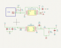
I am designing a programmable output voltage buck converter using the TPS563300, and I would like to request a schematic review to ensure my feedback implementation using a digital potentiometer is correct and stable.
Design summary:
I²C configuration:
I would greatly appreciate any feedback or suggested improvements.
Thank you.
I am designing a programmable output voltage buck converter using the TPS563300, and I would like to request a schematic review to ensure my feedback implementation using a digital potentiometer is correct and stable.
Design summary:
- Buck converter IC: TPS563300
- Input voltage: 20 V
- Output voltage: Target ~5 V (programmable via I²C)
- Controller: MCU (3.3 V I²C)
- Digital potentiometer: MCP4561-503 (50 kΩ, I²C) powered from 5 V
- Top resistor: 52.3 kΩ from VOUT to FB
- Bottom resistor: MCP4561 used in rheostat mode
- P0A → FB
- P0W → FB
- P0B → GND
I²C configuration:
- Pull-ups: 4.7 kΩ to 3.3 V
- MCP4561 powered from 5 V
- Common ground between MCU and power section
- Is using the MCP4561 in this configuration (P0A and P0W tied to FB, P0B to GND) correct and safe for the TPS563300 feedback loop?
- Are there any stability concerns when using a digital potentiometer in the feedback path?
- Should I add a feedforward capacitor (for example, 22–47 pF) across the upper feedback resistor?
- Are there any layout precautions I should follow for noise and stability?
- Is powering the digital pot at 5 V while using 3.3 V I²C pull-ups acceptable?
I would greatly appreciate any feedback or suggested improvements.
Thank you.
Attachments
-
 11.6 KB Views: 8