Building a DIY Regulated Buck Converter using no ICs

Irving

Joined Jan 30, 2016
5,174
I have taken your advice and help into consideration and i now how the following circuit that i attached. It seems to be working decently but i still am unable to achieve 5V exactly and a method to change the duty cycle is evading me since the voltage output of that opamp is not changing with time and hence not affecting pin 5 and the duty cycle doesnt change. Any idea on what could be the issue here?
Look carefully at how you have your output voltmeter connected.

Part of your problem is that the input to your opamp exceeds it's common mode voltage. Look that up and it's effect on opamp functioning. As a suggestion, try scrapping all the various batteries and power everything from the input source. That's how it would be done in reality and avoids problems with things running out of range.
 

Irving

Joined Jan 30, 2016
5,174
Going back to your original question "can you build a buck converter without ICs", the answer is yes, easily, but you then threw in a bunch of ICs which coloured your thinking. Now you're chasing issues created, to some extent, by the complexity of where you've got to. If you were one of my students I'd say go back to 1st principles and consider 2 questions:
1. What's the absolute simplest way to turn the MOSFET on?
2. Having done that, what's the absolute simplest way to turn it off again, without changing the answer to #1.
 

BobTPH

Joined Jun 5, 2013
11,570
You can build a bang-bang converter using only a comparator, voltage reference, MOSFET, diode, inductor and capacitor.

The voltage reference can be two resistors if power in is regulated.
 

Motanache

Joined Mar 2, 2015
652
"can you build a buck converter without ICs", the answer is yes, easily, but you then threw in a bunch of ICs which coloured your thinking.
He probably meant without a dedicated SMPS IC.
I understand that it is an exercise in which he must use the two mentioned 555+ operational amplifier/comparator to create a circuit..
 

MrAl

Joined Jun 17, 2014
13,724
I have taken your advice and help into consideration and i now how the following circuit that i attached. It seems to be working decently but i still am unable to achieve 5V exactly and a method to change the duty cycle is evading me since the voltage output of that opamp is not changing with time and hence not affecting pin 5 and the duty cycle doesnt change. Any idea on what could be the issue here?
Hi,

The connections used in your circuit with the 555 timer IC allows the frequency to change with a variation in the applied CV voltage as well as the desired change in pulse width. The change in frequency is generally not desirable in a switching converter because of the way the ripple changes and may also bother the stability. If that is a problem then you'd have to look for a better design. If not a problem then that's fine once you get all the issues straightened out.

If you can use a dual 555 you can use one section to generate the frequency and the other section to vary only the duty cycle using the applied CV voltage and the frequency will stay constant.

I'm not sure if you meant you can only use one 555 timer IC with just one section, or you could use one 555 timer IC with two sections, or any other parts.

The normal way to provide feedback is with an op amp set up basically as an integrator possibly with some slight variations. The idea is to integrate the error before using it to vary the pulse width, and that provides for a low error in the output setting over as wide range of operating conditions. A typical integrator has at least some capacitance between the output of the op amp and the inverting input although there's a little more to it than that.
 

Thread Starter

RebelliousResistor

Joined Mar 18, 2025
18
Thanks to the help of all of you amazing people I feel i am now almost at the finish line. This is my latest circuit (attached), all i need now is some short circuit or overcurrent protection. I am looking into a current sensor circuit for that (however if you see an easier way for me to do it please advise me). And for some reason my output voltage is bouncing between 4.98 and 5. How would i solve that, im sure its with some capacitor... but where?
 

Attachments

Thread Starter

RebelliousResistor

Joined Mar 18, 2025
18
Edit: also howcome my output current is so extremely low? Is there any way for me to increase it or should i leave it as is, note that this is going to the supply to the other sub system and it was specified that it shouldnt pass 0.5A.
 

Ian0

Joined Aug 7, 2020
13,158
C3 and R3 are ruining the efficiency. You need that MOSFET to switch on and off as fast as possible, within nanoseconds, and you are introducing a delay of a tenth of a second. C3 should not be there at all, and R3 should be less than 30Ω
Also, you STILL don't have enough gate voltage. You need the gate to be 10V ABOVE the SOURCE, otherwise you will lose a lot of power in the MOSFET.
And you STILL don't have a compensation capacitor on the error amplifier, which you have made considerably more difficult by introducing the transistor which swaps the phase.
 

Irving

Joined Jan 30, 2016
5,174
Edit: also howcome my output current is so extremely low? Is there any way for me to increase it or should i leave it as is, note that this is going to the supply to the other sub system and it was specified that it shouldnt pass 0.5A.
Try putting a sensible load resistor on there 5v @ 0.5A = ?Ohm. You can't magically create an output current, you have to draw it out of the system. This is basic electricity 101.

I get you are a beginner, and we all have to start somewhere, but you are compounding your issues by not thinking things through and making silly little mistakes, or not taking ALL the advice onboard (though I'll give you, with so many voices responding, it can be a little confusing) - at the end of the day, this is "Homework Help" not "Homework Do".

all i need now is some short circuit or overcurrent protection. I am looking into a current sensor circuit for that (however if you see an easier way for me to do it please advise me)
Which adds another IC you probably don't have. Again go back to basics... what is the most basic way of determining how much current flows in a circuit, and what is the simplest device that will respond to that?
 

MrAl

Joined Jun 17, 2014
13,724
Thanks to the help of all of you amazing people I feel i am now almost at the finish line. This is my latest circuit (attached), all i need now is some short circuit or overcurrent protection. I am looking into a current sensor circuit for that (however if you see an easier way for me to do it please advise me). And for some reason my output voltage is bouncing between 4.98 and 5. How would i solve that, im sure its with some capacitor... but where?
Hi,

Several things right off the bat.

First, the capacitor connected to the gate of the MOSFET. That's got to go. One of the drawbacks to any MOSFET is the gate capacitance, often referred to as the gate charge, which is always a problem in getting the MOSFET to switch fast enough to keep the efficiency high enough and also NOT burn out the MOSFET. That's quite important, especially with such a larger cap like 1uf. That has to be removed.

Second, as I was saying earlier, the configuration of the 555 looks like it is wired up for a pulse position oscillator, which for the 555 means it's a combination of a pulse position oscillator and a pulse width oscillator. That could cause all kinds of problems, the most serious would be stability, but second would be the variation in the output ripple, and third but not least the gain of the 555 itself. The 555 will have a certain gain in the realm of switching converters, and if the gain is too low, there will be little or no voltage regulation. In a normal PWM oscillator, the PWM switcher would have the pulse width proportional to the input signal voltage. That means the gain is dependent only on the relative ratio of the input voltage to the output pulse width. Because this is not actually a PWM configuration, we could see, as an extreme example, the pulse width and the frequency both vary in the same proportion, which could mean the 555 would have a gain of exactly zero. With a gain of zero, there would be no voltage regulation at all because as the input signal changed the output PWM would maintain the same pulse width to frequency ratio. For a quick example, say 1v input produced a pulse width of 2ms at a frequency of 100Hz. When we raise the input to 2v, the pulse width goes to 1ms, but the frequency goes to 200Hz. Now in the first case we had 2ms at 100Hz, so that means the off time would be 8ms, so the ratio of on time to off time would be 2/8 or 25 percent. In the second case, we had 1ms at 200Hz, so that means the off time would be 4ms, and so the ratio of on time to off time is 1/4 which is still 25 percent. That would mean we ended up with a gain of zero which can not help to regulate the output voltage at all. Hopefully is it not that bad, but it should at least be looked into in order to get an idea what issues that would cause, even if it was not as bad as that extreme example. If the gain of the 555 is too low, it would take an input voltage swing that is too large for the converter to work as is.

I think I like the idea of the 2N2222 transistor though, that could work, although it does introduce more nonlinearities which could be a problem again. We want the input voltage to pulse width to be as linear as possible, but some nonlinearity is acceptable as I have seen in past converters. Maybe the gain of the transistor could be partly linearized a little by added some resistors.

It's too bad you did not answer yet about using the dual section 555 or even two separate 555 timer IC's used together to create a real PWM section. That would put it more in line with many of the past PWM regulators like the buck regulator and would ensure success with less analytics and less bench testing. This design has to be checked carefully on the bench as well as in simulation.

Again, I am not entirely sure what kind of parts you can use, but using two comparators you can create a true PWM regulator that is very good linearity. It's a relatively simple circuit too. That would NOT include a 555 timer though, so I have a feeling you would not be allowed to do that.

I almost forgot, if the gain of the PWM section is too low then there is a risk that the CV voltage will go out of range and lock up the PWM signal. With that 2N2222 transistor that should not happen though, but with that you also lose some PWM adjustment range. I have a feeling the transistor will be ok though, as long as the linearity issues do not bother the overall regulation of the converter.
 
Last edited:

MrAl

Joined Jun 17, 2014
13,724
Hello again,

I did a quick study of the duty cycle change with applied CV voltage and also the frequency change for the astable 555 with CV voltage control which is what is being used in this circuit so far.
The duty cycle comes out close to linear, while the frequency changes by about 2.5 to 1 as the voltage changes.

The plot for the Duty Cycle is shown in one pic, the Duty Cycle combined with the scaled Frequency is shown in the other pic.
Both of these plots are done with Vcc=10v, and CV runs from 1v to 7.5v because that's a good set of limits for this chip. For voltages other than Vcc=10v simply scale the input by the same as the changed Vcc voltage. That simply means that at Vcc=5v for example the input of 2v on the plot would now be just 1v, and 1v would be 0.5v, etc. This in turn means the x axis can be read off as percent of Vcc if we multiply all of those voltages by 10. That would put the range of input from 10 percent to 75 percent of Vcc which is a good limit for the CV input.

The duty cycle range tells us that it should be OK for a buck converter, but the frequency change tells us that the ripple will change drastically on the output, and the transistor will have to be able to switch at 2.5 times the lowest frequency. That kind of characteristic is not desirable in a converter, but it could work anyway as long as everything else works ok. I would guess that it would be a bust in a modern circuit though because harmonics are a concern these days with the associated EMR.
 

Attachments

Last edited:

Thread Starter

RebelliousResistor

Joined Mar 18, 2025
18
Hi,

Several things right off the bat.

First, the capacitor connected to the gate of the MOSFET. That's got to go. One of the drawbacks to any MOSFET is the gate capacitance, often referred to as the gate charge, which is always a problem in getting the MOSFET to switch fast enough to keep the efficiency high enough and also NOT burn out the MOSFET. That's quite important, especially with such a larger cap like 1uf. That has to be removed.

Second, as I was saying earlier, the configuration of the 555 looks like it is wired up for a pulse position oscillator, which for the 555 means it's a combination of a pulse position oscillator and a pulse width oscillator. That could cause all kinds of problems, the most serious would be stability, but second would be the variation in the output ripple, and third but not least the gain of the 555 itself. The 555 will have a certain gain in the realm of switching converters, and if the gain is too low, there will be little or no voltage regulation. In a normal PWM oscillator, the PWM switcher would have the pulse width proportional to the input signal voltage. That means the gain is dependent only on the relative ratio of the input voltage to the output pulse width. Because this is not actually a PWM configuration, we could see, as an extreme example, the pulse width and the frequency both vary in the same proportion, which could mean the 555 would have a gain of exactly zero. With a gain of zero, there would be no voltage regulation at all because as the input signal changed the output PWM would maintain the same pulse width to frequency ratio. For a quick example, say 1v input produced a pulse width of 2ms at a frequency of 100Hz. When we raise the input to 2v, the pulse width goes to 1ms, but the frequency goes to 200Hz. Now in the first case we had 2ms at 100Hz, so that means the off time would be 8ms, so the ratio of on time to off time would be 2/8 or 25 percent. In the second case, we had 1ms at 200Hz, so that means the off time would be 4ms, and so the ratio of on time to off time is 1/4 which is still 25 percent. That would mean we ended up with a gain of zero which can not help to regulate the output voltage at all. Hopefully is it not that bad, but it should at least be looked into in order to get an idea what issues that would cause, even if it was not as bad as that extreme example. If the gain of the 555 is too low, it would take an input voltage swing that is too large for the converter to work as is.

I think I like the idea of the 2N2222 transistor though, that could work, although it does introduce more nonlinearities which could be a problem again. We want the input voltage to pulse width to be as linear as possible, but some nonlinearity is acceptable as I have seen in past converters. Maybe the gain of the transistor could be partly linearized a little by added some resistors.

It's too bad you did not answer yet about using the dual section 555 or even two separate 555 timer IC's used together to create a real PWM section. That would put it more in line with many of the past PWM regulators like the buck regulator and would ensure success with less analytics and less bench testing. This design has to be checked carefully on the bench as well as in simulation.

Again, I am not entirely sure what kind of parts you can use, but using two comparators you can create a true PWM regulator that is very good linearity. It's a relatively simple circuit too. That would NOT include a 555 timer though, so I have a feeling you would not be allowed to do that.

I almost forgot, if the gain of the PWM section is too low then there is a risk that the CV voltage will go out of range and lock up the PWM signal. With that 2N2222 transistor that should not happen though, but with that you also lose some PWM adjustment range. I have a feeling the transistor will be ok though, as long as the linearity issues do not bother the overall regulation of the converter.
Thank you so much for taking the time to give me such a detailed explanation and help with this circuit. I will be implementing these changes asap. You know how engineering is theres so much going on and you can never just focus on one thing. But i will get to this right away :)
 

Thread Starter

RebelliousResistor

Joined Mar 18, 2025
18
Hi,

Several things right off the bat.

First, the capacitor connected to the gate of the MOSFET. That's got to go. One of the drawbacks to any MOSFET is the gate capacitance, often referred to as the gate charge, which is always a problem in getting the MOSFET to switch fast enough to keep the efficiency high enough and also NOT burn out the MOSFET. That's quite important, especially with such a larger cap like 1uf. That has to be removed.

Second, as I was saying earlier, the configuration of the 555 looks like it is wired up for a pulse position oscillator, which for the 555 means it's a combination of a pulse position oscillator and a pulse width oscillator. That could cause all kinds of problems, the most serious would be stability, but second would be the variation in the output ripple, and third but not least the gain of the 555 itself. The 555 will have a certain gain in the realm of switching converters, and if the gain is too low, there will be little or no voltage regulation. In a normal PWM oscillator, the PWM switcher would have the pulse width proportional to the input signal voltage. That means the gain is dependent only on the relative ratio of the input voltage to the output pulse width. Because this is not actually a PWM configuration, we could see, as an extreme example, the pulse width and the frequency both vary in the same proportion, which could mean the 555 would have a gain of exactly zero. With a gain of zero, there would be no voltage regulation at all because as the input signal changed the output PWM would maintain the same pulse width to frequency ratio. For a quick example, say 1v input produced a pulse width of 2ms at a frequency of 100Hz. When we raise the input to 2v, the pulse width goes to 1ms, but the frequency goes to 200Hz. Now in the first case we had 2ms at 100Hz, so that means the off time would be 8ms, so the ratio of on time to off time would be 2/8 or 25 percent. In the second case, we had 1ms at 200Hz, so that means the off time would be 4ms, and so the ratio of on time to off time is 1/4 which is still 25 percent. That would mean we ended up with a gain of zero which can not help to regulate the output voltage at all. Hopefully is it not that bad, but it should at least be looked into in order to get an idea what issues that would cause, even if it was not as bad as that extreme example. If the gain of the 555 is too low, it would take an input voltage swing that is too large for the converter to work as is.

I think I like the idea of the 2N2222 transistor though, that could work, although it does introduce more nonlinearities which could be a problem again. We want the input voltage to pulse width to be as linear as possible, but some nonlinearity is acceptable as I have seen in past converters. Maybe the gain of the transistor could be partly linearized a little by added some resistors.

It's too bad you did not answer yet about using the dual section 555 or even two separate 555 timer IC's used together to create a real PWM section. That would put it more in line with many of the past PWM regulators like the buck regulator and would ensure success with less analytics and less bench testing. This design has to be checked carefully on the bench as well as in simulation.

Again, I am not entirely sure what kind of parts you can use, but using two comparators you can create a true PWM regulator that is very good linearity. It's a relatively simple circuit too. That would NOT include a 555 timer though, so I have a feeling you would not be allowed to do that.

I almost forgot, if the gain of the PWM section is too low then there is a risk that the CV voltage will go out of range and lock up the PWM signal. With that 2N2222 transistor that should not happen though, but with that you also lose some PWM adjustment range. I have a feeling the transistor will be ok though, as long as the linearity issues do not bother the overall regulation of the converter.
Yes it would absolutly be allowed. I will be allowed 2 555 timer ICs. The only restriction is that there can not be any smps IC, so the amount of 555 timers and op amps would not be an issue
 

Thread Starter

RebelliousResistor

Joined Mar 18, 2025
18
Hi,

Several things right off the bat.

First, the capacitor connected to the gate of the MOSFET. That's got to go. One of the drawbacks to any MOSFET is the gate capacitance, often referred to as the gate charge, which is always a problem in getting the MOSFET to switch fast enough to keep the efficiency high enough and also NOT burn out the MOSFET. That's quite important, especially with such a larger cap like 1uf. That has to be removed.

Second, as I was saying earlier, the configuration of the 555 looks like it is wired up for a pulse position oscillator, which for the 555 means it's a combination of a pulse position oscillator and a pulse width oscillator. That could cause all kinds of problems, the most serious would be stability, but second would be the variation in the output ripple, and third but not least the gain of the 555 itself. The 555 will have a certain gain in the realm of switching converters, and if the gain is too low, there will be little or no voltage regulation. In a normal PWM oscillator, the PWM switcher would have the pulse width proportional to the input signal voltage. That means the gain is dependent only on the relative ratio of the input voltage to the output pulse width. Because this is not actually a PWM configuration, we could see, as an extreme example, the pulse width and the frequency both vary in the same proportion, which could mean the 555 would have a gain of exactly zero. With a gain of zero, there would be no voltage regulation at all because as the input signal changed the output PWM would maintain the same pulse width to frequency ratio. For a quick example, say 1v input produced a pulse width of 2ms at a frequency of 100Hz. When we raise the input to 2v, the pulse width goes to 1ms, but the frequency goes to 200Hz. Now in the first case we had 2ms at 100Hz, so that means the off time would be 8ms, so the ratio of on time to off time would be 2/8 or 25 percent. In the second case, we had 1ms at 200Hz, so that means the off time would be 4ms, and so the ratio of on time to off time is 1/4 which is still 25 percent. That would mean we ended up with a gain of zero which can not help to regulate the output voltage at all. Hopefully is it not that bad, but it should at least be looked into in order to get an idea what issues that would cause, even if it was not as bad as that extreme example. If the gain of the 555 is too low, it would take an input voltage swing that is too large for the converter to work as is.

I think I like the idea of the 2N2222 transistor though, that could work, although it does introduce more nonlinearities which could be a problem again. We want the input voltage to pulse width to be as linear as possible, but some nonlinearity is acceptable as I have seen in past converters. Maybe the gain of the transistor could be partly linearized a little by added some resistors.

It's too bad you did not answer yet about using the dual section 555 or even two separate 555 timer IC's used together to create a real PWM section. That would put it more in line with many of the past PWM regulators like the buck regulator and would ensure success with less analytics and less bench testing. This design has to be checked carefully on the bench as well as in simulation.

Again, I am not entirely sure what kind of parts you can use, but using two comparators you can create a true PWM regulator that is very good linearity. It's a relatively simple circuit too. That would NOT include a 555 timer though, so I have a feeling you would not be allowed to do that.

I almost forgot, if the gain of the PWM section is too low then there is a risk that the CV voltage will go out of range and lock up the PWM signal. With that 2N2222 transistor that should not happen though, but with that you also lose some PWM adjustment range. I have a feeling the transistor will be ok though, as long as the linearity issues do not bother the overall regulation of the converter.
The 555 timer is not a "must have" i only opted to use it becuase we learnt about it recently in class
 

MrAl

Joined Jun 17, 2014
13,724
The 555 timer is not a "must have" i only opted to use it becuase we learnt about it recently in class
Hi again,

Oh ok, well now that I think about it, I probably should not 'dictate' what you should use because that's probably supposed to be your idea, but if you think it is ok you could use two 555's to get a decent PWM buck regulator probably without too much trouble. Alternately, a couple comparators.

Do you have a target switching frequency in mind?
 

Thread Starter

RebelliousResistor

Joined Mar 18, 2025
18
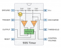
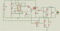
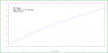
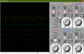
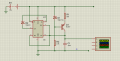
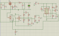
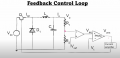
Alright i have checked with some of my mentors and they advised me against using the method that i am currently using since the efficiency is so terrible. They have brought my attention to using the 555 timer as a sawtooth wave generator and using a comparator to create the pwm for the switching of the MOSFET. I may not be communicating this well so ill attach a picture of the diagrams (in the first page of the pdf that i sent) this pdf seems to have a detailed circuit with the exact specifications of my project, even including the calculated component values and even compensation for the op amp. However when i connect it on my own I'm not getting the same result? I have also attached a similar image of the concept. I suspect the MOSFET selection or something might be an issue since I'm not very experienced with it. Ill also attach the 555 timer circuit i am using to generate the sawtooth wave for Vramp. And ill attach my schematic that i currently have on proteus (Modelled after the one in the pdf i attached). Also it would help me a great deal if you could explain the switching frequency correlation with the frequency of this ramp because im taking a switching frequency of 100kHz. Does it need to be the same for the ramp or does it not matter? In my head its got to be the same right. 1746131957700.png1746131792683.png1746131705332.png1746130988124.png
 

Attachments

Thread Starter

RebelliousResistor

Joined Mar 18, 2025
18
Hi again,

Oh ok, well now that I think about it, I probably should not 'dictate' what you should use because that's probably supposed to be your idea, but if you think it is ok you could use two 555's to get a decent PWM buck regulator probably without too much trouble. Alternately, a couple comparators.

Do you have a target switching frequency in mind?
Is my new idea the comparator idea that you had, i chose my switching frequency to be 100kHz
 
Top