AS3340 PCB layout. Major stability issue in oscillation.

Thread Starter

gottman4

Joined Oct 30, 2019
8
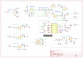
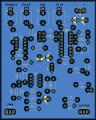
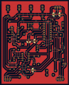
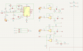
Hi! I've made my own PCB layout, that I've etched my self. The circuit works on breadboard but once i made the PCB there are major fluctuations in the oscillation. I power it on and it oscillates at around 16kHz to then every now and then dip down to a more audible range but its very "jittery". If i touch the connections between R5 and R20 with my finger the frequency *sometimes* dips down to a more audible range, but the stability of the frequency is terrible and very chaotic.

I've looked over the connections and made sure there are no shorts or cold solder joints and also cross-referenced the circuit with both the as3340 data sheet and other known as3340 circuits but i can't find any discrepancies.

I am aware that the issue might lay in the quality of my homemade PCB but I haven't found any issues in my measurements yet.

I'm more doing this as a sanity check at this point. Does anyone see any issues in the PCB layout or schematic? Any help or suggestions to potential issues is much appreciated.

I'm using a Mean Well RD-3513 set to 12volt as my power supply and have ensured that the +/- is set to the correct terminals.

Thank you!
 

Attachments

ronsimpson

Joined Oct 7, 2019
4,646
Add cap from pin 16 to 12 very close to the part.
1760370589393.png
Normally we do not have unconnected copper on the board. I don't know if that is one of the problems. Everywhere there are floating pieces of RED copper.
Next time: 1) Name the RED copper GROUND. 2) Set the CAD program to not have floating copper. 3) put a VIA from the RED side to the other side to at least connect them to ground. 4) Reduce the clearance to 1/2 of what it is. This will help make Ground stronger and will connect more of the RED together.
I think these areas are loosely connecting signals together that should not be connected.
1760370702280.png
The PCB with copper on both sides makes small capacitors. (plate/insulator/plate is a capacitor) I tried to show how these capacitors connect the left trace to the topside and back to the bottom right trace.
1760371224926.png
 

ronsimpson

Joined Oct 7, 2019
4,646
I don't know this IC but I have done this type of work from 1965.
By looking the schematic, I see that Pin-13 and Pin 15 are very sensitive to noise. Touching them with your finger will drive the IC insane. I put red dots on the copper traces that need to be very short. (the layout has very long traces)
Put R4, R5, right up against Pin-13. Keep R20 close to R5.
Put R10, R9, R3, R2 close to Pin-15. Keep the amount of copper small.
Having these traces with floating copper over the top is not good.
1760371876108.png
I do not know about Pin-1 and Pin-2. I would need to learn about the IC.
---edited---
Pins-1&2 should be short connections. You could use smaller wattage resistors.
 
Last edited:

panic mode

Joined Oct 10, 2011
4,864
your circuit is apparently different from any other schematic for that IC:
pins 1 and 2 of RV1 are swapped.
and for some reason you added R3.
pullup on pin 15 is sometimes present but the values is high (360k) that is higher than R10 and RV3 can ever be.
 

Thread Starter

gottman4

Joined Oct 30, 2019
8
Add cap from pin 16 to 12 very close to the part.
View attachment 357095
Normally we do not have unconnected copper on the board. I don't know if that is one of the problems. Everywhere there are floating pieces of RED copper.
Next time: 1) Name the RED copper GROUND. 2) Set the CAD program to not have floating copper. 3) put a VIA from the RED side to the other side to at least connect them to ground. 4) Reduce the clearance to 1/2 of what it is. This will help make Ground stronger and will connect more of the RED together.
I think these areas are loosely connecting signals together that should not be connected.
View attachment 357096
The PCB with copper on both sides makes small capacitors. (plate/insulator/plate is a capacitor) I tried to show how these capacitors connect the left trace to the topside and back to the bottom right trace.
View attachment 357097

Very, very interesting! Sounds like a big revision is needed. I am very early into the learning pcb design so it's always something new i've missed.

Interesting with the capacitance of the copper. So if this was a single layered board; would this not be an issue given it dosen't have two opposing copper layers?
 

ronsimpson

Joined Oct 7, 2019
4,646
Interesting with the capacitance of the copper. So if this was a single layered board; would this not be an issue given it dosen't have two opposing copper layers?
If the RED copper was ground, there would be very little connection between traces.
Capacitance = ( Type of insulator X copper area / distance between plates)
Two BLUE traces running in parallel, the area is the length of the trace X thickness of copper. Because the thickness is very small the capacitor is very small.
The capacitance of a blue trace to a red plane is large because the area of Blue is length X width of trace.

Some of the very important traces are 4 inches long, when they should be 0.4" long.
Did you see that panic mode has questions about the schematic?

Normally there should be a capacitor from -12V to ground and +12V to ground at each opamp.
 
Last edited:

Thread Starter

gottman4

Joined Oct 30, 2019
8
your circuit is apparently different from any other schematic for that IC:
pins 1 and 2 of RV1 are swapped.
and for some reason you added R3.
pullup on pin 15 is sometimes present but the values is high (360k) that is higher than R10 and RV3 can ever be.

Oh yeah, you're right. Completely missed RV3.

regarding R3 I've picked parts of another existing schematic (se attached file). I wanted a schematic that was made for 12v +/- instead of the 15v that the data sheet is adjusted to. I added R3 to get closer to the value of 2M2 that is present in the reference schematic I've attached, since i didn't have a 2M2 resistor on hand i figured 2M would be close enough. Maybe that was a bit of a shortcut but it worked alright when i breadboarded it. Not a lot of thought was but in to that decision tho since I struggle to understand the exact function of that resistor.

The pull up resistor on pin 15 seems to be somewhat optional since it varies alot between diffrent schematics if its used or not, like you said. I think it's mainly used to bias the lowest possible frequency on the chip, since pin 15 is the frequency control input.

If you could help me understand it it would be much appreciated!

Thank you for the response!
 

Attachments

Top