Facebook
 Google
 GitHub
 Linkedin
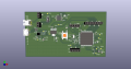
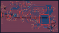
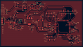
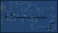
To add some context to this PCB layout, it's a four-layer board with a signal/ground/ground/signal stack-up. Since the inner layers are just reference planes, I didn't add any tracks and didn't see the need to include pictures of them. I used 0.4 mm tracks for nets that needed 5V, 0.3 mm for nets with 3.3V, and 0.2 mm for signals.
My main concern lies in the Micro-B USB connector's data lines and the layout of the J6 and J7 header pins. I added those two headers as a backup option in case the slide switch malfunctions. However, I'm not sure if current would still flow through the switch if it's already shorted.
I would appreciate it if anyone can point out any obvious problems that I may have missed.
Attachments
-
 175.8 KB Views: 12
 -
 43.5 KB Views: 12
 -
 180.9 KB Views: 10
 -
 160.3 KB Views: 9
 -
 70.6 KB Views: 9