555 voltage booster

MisterBill2

Joined Jan 23, 2018
27,530
The brain fog and lack of notebook is really eating my lunch, the second figure is my attempt to redraw the first:
would someone please proof the schematics please?
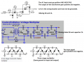
The circuit matches, but the error is that two things, (D1 and C2) are grounded instead of being connected to the line from input common to output common. YES, I AM rather picky about that sort of thing. I will be the first to admit it. That is because it matters. In this drawing we need to assume that both input and output are referenced to "ground", which is not always the case.
 

MisterBill2

Joined Jan 23, 2018
27,530
Thank you, isn't this a ground?
In this drawing it is a round connection, BUT in the drawing that W was asking us to verify there was no actual indication that the input or output were referenced to ground. It was only presumed.
And the whole thing looks a bit "off" because resistor R1 is connected between two identical ground symbols.
In addition, consider that the TS had expressed concern previously that the return side of the output was not commoned with the return side of the power input source, which was an initial requirement.
 

Thread Starter

Wendy

Joined Mar 24, 2008
23,798
I'm looking forward to playing with this, I have to wonder if D5 and C5 are necessary? Time will tell.
00.png
 

Papabravo

Joined Feb 24, 2006
22,082
Be prepared for the voltage to drop if you try to draw "too much" current out of the 15V point. I'd suggest starting with a LED current of 2 mA or so.
 

Audioguru again

Joined Oct 21, 2019
6,826
In post #1 the 555 output goes to 0V (ground) and to +5V. It never goes negative.
The transformer output goes positive and negative with ground in the middle.

The literature shows 4 diodes and 4 capacitors in a two-stage multiplier then I show 6 diodes and 6 capacitors in a three stage multiplier.
 

Attachments

Audioguru again

Joined Oct 21, 2019
6,826
C1 charges thru D1 only when the input signal goes negative.
When the input signal goes positive, C2 charges thru D2 from the charged voltage on C1 plus the input voltage.
Minus the low forward voltages of the Schottky diodes.
 

Thread Starter

Wendy

Joined Mar 24, 2008
23,798
I don't think that is a supportable position, but you're entitled to it. It does affect my opinion of your credibility on a whole range of other things.
In post #1 the 555 output goes to 0V (ground) and to +5V. It never goes negative.
The transformer output goes positive and negative with ground in the middle.

The literature shows 4 diodes and 4 capacitors in a two-stage multiplier then I show 6 diodes and 6 capacitors in a three stage multiplier.
So the highlighted schematic is flawed, I had not realized that I needed a balanced signal. Which means I will need qty2 555 circuits to drive it. So I will go with this schematic:

Temp1.png
now the question is where can I tap the outputs for voltages:

Temp2.png

would this assumption be correct?

Temp3.png
 
Last edited:

Thread Starter

Wendy

Joined Mar 24, 2008
23,798
I probably screwed up on orienting the mosfets, but I am hoping folks on this site will correct me if I got it wrong funny thing is I don't even know if I have these parts I plan on ordering ordering them via Amazon if I don't (of course the mosfets are logic level devices):
#5.png
 
Last edited:

Papabravo

Joined Feb 24, 2006
22,082
The symbols show an N-Channel and a P-Channel, but I think you have them in the wrong place and the P-Channel device is in the wrong orientation. Also, your gate resistor R2 at 10K is way too large. There is no DC current that flows in and out of the gate. The following shows the correct way to draw a complementary MOSFET push-pull driver. I tried to find logic level devices, but the p-channel device has a pretty large rds(on) at 6.25Ω
1658273515704.png
 
Last edited:

Thread Starter

Wendy

Joined Mar 24, 2008
23,798
Thank you very much. So it should look more like this?

#5.png

that is if I didn't make another brain fart, no one's complained about the smell yet.
 
Last edited:

Papabravo

Joined Feb 24, 2006
22,082
You still need to make the resistors labeled R2 smaller than 10K. You want to switch the gate as rapidly as possible, and the small resistance is to damp any ringing that might be produced.
 

Thread Starter

Wendy

Joined Mar 24, 2008
23,798
Studying this I realized I had got the transistors wrong yet again:

#5.png

Now to layout the protoboard.
 

BobTPH

Joined Jun 5, 2013
11,516
That circuit will triple 2.5V, which is the RMS voltage of the input. I have been playing with this in LTSPICE.

To triple a 5V square wave, you need to build the multiplier on top of the 5V supply, like this:

1658333625145.png

Here, I have tripled the 5V input and got out about 13V at 13mA.
 

Papabravo

Joined Feb 24, 2006
22,082
That circuit will triple 2.5V, which is the RMS voltage of the input. I have been playing with this in LTSPICE.

To triple a 5V square wave, you need to build the multiplier on top of the 5V supply, like this:

View attachment 271871

Here, I have tripled the 5V input and got out about 13V at 13mA.
Works better if you use Schottky diodes instead of signal diodes.
 
Top