Facebook
 Google
 GitHub
 Linkedin
Jon Chandler
- Joined Jun 12, 2008
- 1,620
*shrug* I don't know. This is your board to lay out. I have explained in several different ways why the DC-025:is an extremely poor choice. I have explained why I have made various suggestions several times but you're just not getting it.
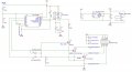
I have drawn you a schematic that includes almost all the parts except for the DC power jack and headers (which I have suggested separately) – parts with full details and footprints which are in stock in JLC's assembly program. All you have to do is click the button to dump the footprints on onto the board arrange them and route tracks. I even suggested a specific video tutorial that shows how to use the exact same software to lay out a board.
Have you even attempted to try to lay out a board? Move the parts around to see how it works? Done anything beyond opening the software?
I have spent many hours to help you get to a place where you would have a good chance to make a nice solution. But it seems you don't want help to learn how to do this – you want someone to turn your ill-defined ideas into reality. I have solved many issues for you that you hadn't even considered.
I don't care how big your board is. I don't care where you position parts. It's not MY project. It's not MY board. I have tried to help. I have said no more, then felt guilty for not providing every f$%&^ detail. But now I just feel stupid.
If you can't do this yourself after almost ALL OF IT has been done for you, it's time to hire someone and pay them actual money to do it for you. But look for someone to "design and build" rather than just lay out a circuit board using MY WORK. I am certain you have skipped on many of the details.
Time to find another sucker.