Yellow contamination on PCB. Flux? Capacitor leaked?

Thread Starter

Dave Lowther

Joined Sep 8, 2016
347
I wouldn't be taking things off; there's a chance you could damage the board.
I agree. I only removed that daughter board because I knew it wasn't the source of the fault, and I needed to get to the circuitry under it.
I'd just start reflowing the solder joints I can reach AND reliably resolder them one by one. Every so often I'd stop to see if the fault still exists when the board is flexed.
I'd rather reverse engineer the part of that's common to all 3 inputs / all 3 outputs, at least to some extent. It's not just about fixing this fault, I'm also interested in having more info on how it's been designed.
There's a good chance the fracture may very well have been between the daughter and mother board.
I thought so too, and reflowed the solder on the 3 way header connections on both boards, but that didn't fix it.
 

MisterBill2

Joined Jan 23, 2018
27,997
I have reflowed every solder joint in a Kenwood stereo amplifier in about 15 minutes. During my lunch break. That was the fix, it had quite a few poor solder connections. Rather then evaluate and investigate, redoing every one is much faster. Have a hot iron and move quickly.
 

Thread Starter

Dave Lowther

Joined Sep 8, 2016
347
I have reflowed every solder joint in a Kenwood stereo amplifier in about 15 minutes. During my lunch break. <snip>. Have a hot iron and move quickly.
I've made my own PCBs, with one chip the same size as the opamps on this board, but I've never done any work on such small components as the SMD resistors and capacitors on this board. I have a desk magnifying lamp that I'm using, but even with that my eyesight isn't great these days.
I'm concerned that I might do more harm than good if I just reflow everything. I'm worried that I might heat one of those small components enough to melt the solder on both ends, and the component might move out of place or fall off.
I'm not sure what 'reflow' means exactly in this context. I have Googled. Should I just used a tinned soldering iron, or do I have to add more solder? If the latter, can I use fine multi-core solder, or should I be using solder paste?
As I said in post #21, I'm finding it interesting to reverse engineer the PCB to get a circuit diagram. I'm enjoying myself. I'm retired. This is my hobby. I'd be much more satisfied if I could locate the fault, rather than fixing it without knowing where the fault was.
 

Tonyr1084

Joined Sep 24, 2015
9,744
I'm not sure what 'reflow' means exactly in this context.
Reflow means exactly that - to heat the solder to molten state where it will re-flow to the component and the board.
Should I just used a tinned soldering iron, or do I have to add more solder? If the latter, can I use fine multi-core solder, or should I be using solder paste?
I'd suggest fluxing the component with flux. I haven't a good suggestion as to what kind of flux, I'll let others answer that part, but fluxing the joints and making a good thermal contact with your iron should cause the solder to reflow. Once it reflows you're done. Don't dwell on it because you COULD overheat it and cause the other side to flow as well. You're wise to be concerned about moving parts. That's why you should dwell long enough to just get the solder to flow, then get away from it.
This is my hobby. I'd be much more satisfied if I could locate the fault, rather than fixing it without knowing where the fault was.
Sometimes reflowing everything IS the way to find the fault. You may never know which component it was that was poorly soldered, but knowing which component will not enhance your understanding of the circuit.

If after having reflowed all the joints and nothing has changed then either you have a broken trace (the copper on the PCB) or a component has an internal fracture. To find such a component will take an extensive understanding of the circuit and the ability to test each component. If I had to - I wouldn't be able to. I have a scope and maybe - just maybe - I might find the faulty component. If it should be a chip capacitor such as 3C1 you will not know the value because there is no marking on it to tell you its farad rating or voltage. Fortunately there are many on this website who will likely have a very good idea of what that component value may be.

Good luck with your repair endeavors.
 

Thread Starter

Dave Lowther

Joined Sep 8, 2016
347
Good luck with your repair endeavors.
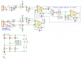
I've reverse engineered the circuit diagram to this extent.
1741359382921.png
Next week I'll inject a signal on CN1 and see if flexing the board makes the output at U2A pin 1 come and go. I hope it does, then I won't have much to reflow. If the fault happens at some point after U2A pin 1, then I'll reconsider my approach.
 

Tonyr1084

Joined Sep 24, 2015
9,744
Just curious: Do the resistors have numbers on them? Something like 201 or 4501 (3 or 4 number sequence will tell the resistor value; 4 numbers means a precision resistor).
 

Tonyr1084

Joined Sep 24, 2015
9,744
This is a PCB from some active speakers. It's the input board which takes the signal from the XLR connector, filters it into 3 bands (woofer, mid, tweeter) and then outputs those 3 signals to the power amplifier board. This board gets its power (+/- 12V) from the power amplifier board. The connector in the above photo is the connector for the power from / outputs to the power amplifier board.
Diagnostics question: Do all three ranges drop out when flexed? Or just one? Or two but not all three?
 

Tonyr1084

Joined Sep 24, 2015
9,744
OK, yes, I can see there ARE markings on the resistors. A clearer picture will tell us what values they are.
Screenshot 2025-03-07 at 8.17.11 AM.png
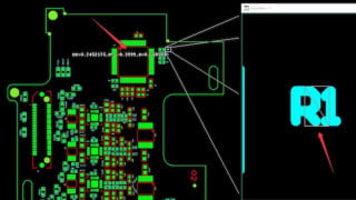
R101 is a 473 resistor. That means it's 47KΩ. How? Why? The first two numbers are values, the third (or last) number is a multiplier (X10). So 473 = 47,000 (three zeros).
R147 "Appears" to be 912. If I'm reading that right it would be a 9.1KΩ resistor (or 9100Ω - same thing). I've never heard of a 9.1K resistor (which may also be expressed as 9K1 - which also means the same thing).
 

seanstevens

Joined Sep 22, 2009
323
Just a thought, it could also be a cracked SMD capacitor or resistor causing the issue. I have had an SMD cap with a crack which I eventually zeroed in which was very difficult even to see the crack on its surface.
Reflowing the SMD part is not difficult if you have a fine-tipped iron, a large magnifying lamp and lots of patience. You just need to go through every SMD systematically.
 

Thread Starter

Dave Lowther

Joined Sep 8, 2016
347
Diagnostics question: Do all three ranges drop out when flexed? Or just one? Or two but not all three?
Yes all 3 ranges, and the fault is common to all 3 inputs. So it's got to be a fault in the section after the inputs are combined and before the filter sections. Which should be a relatively small section of the board
 

Tonyr1084

Joined Sep 24, 2015
9,744
Yes all 3 ranges, and the fault is common to all 3 inputs.
First two places I'd reflow solder would be U1 and RV1.

Quick question about your schematic. It seems like the inputs are on CN1 & 2. I’m not sure what CLMP-A, B, & C are, and what does U2A do. Where is its output? Does it have an output? I’m not an audio expert, so I might be asking some basic questions. But asking questions, even if they seem dumb, can help us learn and grow.
 

Tonyr1084

Joined Sep 24, 2015
9,744
Looking at the overall board CN3 would be a FIRST good candidate for reflowing the solder joints.

And if you get clearer pictures that may be helpful as well.

On the yellow capacitors - such as 105J100, while I'm not familiar with all the coding, 105 = 1,000,000 Pico Farads, which is also 1,000 Nano Farads, which is also 1 Micro Farad. I'm confident the J is a temperature standard and the 100 may be a reference to its reliability. I think!
 

Thread Starter

Dave Lowther

Joined Sep 8, 2016
347
First two places I'd reflow solder would be U1 and RV1.

Quick question about your schematic. It seems like the inputs are on CN1 & 2. I’m not sure what CLMP-A, B, & C are, and what does U2A do. Where is its output? Does it have an output? I’m not an audio expert, so I might be asking some basic questions. But asking questions, even if they seem dumb, can help us learn and grow.
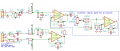
CLMP = my abbreviation for clamp, sorry I missed that part off the screen shot of KiCad. I'd moved the clamping / power supply section well out the way of what I was focussing on. I guess it will be obvious now, but it's protection to stop the inputs going outside the range of the +/- 12V supply to the opamps.
I've not found where the output of U2A goes yet. The large yellow capacitors are making it difficult to trace the tracks. Is seems to be a 4 layer board. I can only get to the terminals of those caps on the underside of the board, but there's no tracks on that side of the board. I find it difficult to probe the top and bottom of the board at the same time.
I think U2A is a buffer for the volume control pot output. It may have some gain too. I won't know until / if I add the resistor values to the diagram.
1741362495044.png
 

Thread Starter

Dave Lowther

Joined Sep 8, 2016
347
Looking at the overall board CN3 would be a FIRST good candidate for reflowing the solder joints.

And if you get clearer pictures that may be helpful as well.

On the yellow capacitors - such as 105J100, while I'm not familiar with all the coding, 105 = 1,000,000 Pico Farads, which is also 1,000 Nano Farads, which is also 1 Micro Farad. I'm confident the J is a temperature standard and the 100 may be a reference to its percentage of accuracy. I think!
CN3 has +/- 12V supply inputs and the outputs for the 3 power amps. So the only part common to all 3 bands is the power supply input. It could be a faulty power supply connection, but I think that if one of the power connections was intermittent it would make some quite loud pops when the fault comes and goes, but it doesn't do that.
I'm not concerned about the values of the yellow capacitors ATM. My, possibly naive, view is that those caps would only be used for filters, and the fault happens before the filters. There may be a common sub-sonic filter, but I'll worry about that if the fault isn't in the common circuitry in post #34
 

Thread Starter

Dave Lowther

Joined Sep 8, 2016
347
Just a thought, it could also be a cracked SMD capacitor or resistor causing the issue. I have had an SMD cap with a crack which I eventually zeroed in which was very difficult even to see the crack on its surface.
Reflowing the SMD part is not difficult if you have a fine-tipped iron, a large magnifying lamp and lots of patience. You just need to go through every SMD systematically.
Thanks for the advice. Hopefully I'll find that the fault is in the common circuitry in post #34. That would narrow down the amount of places I need to reflow.
 

Thread Starter

Dave Lowther

Joined Sep 8, 2016
347
@MrChips @Tonyr1084 Thanks for the info on resistor values. Right now I'm not looking into documenting their values. I recognise the shape of the opamp configurations used in the input circuitry, and that's enough for me to see the signal path. I've designed and built (using through hole components) a preamplifier using opamps based on info I taught myself from reading one of Doug Self's books (small signal design?).
 

skstrobel

Joined Nov 29, 2023
29
Just a thought, it could also be a cracked SMD capacitor or resistor causing the issue. I have had an SMD cap with a crack which I eventually zeroed in which was very difficult even to see the crack on its surface.
Reflowing the SMD part is not difficult if you have a fine-tipped iron, a large magnifying lamp and lots of patience. You just need to go through every SMD systematically.
One advantage of reflowing the SMD parts is that it can help you find cracked resistors and caps. If you heat one end and it falls apart, it was likely already broken and just held together by the solder on the two ends. Of course, once that happens it can be a challenge to figure out the correct replacement part.
 

Tonyr1084

Joined Sep 24, 2015
9,744
Is seems to be a 4 layer board.
Now THAT's scary. Multi-Layered (ML) boards can have internal fractures where you'll never find them. Most common points of failure in ML boards is the inner connections. Thermal expansion and contraction can separate internal traces from internal pads. You can't fix those. But it's still worth reflowing the pins on the connectors. If it's NOT on an inner layer there's a good chance you can rectify the issue.
 
The ceramic cap has a large C value /w low voltage causes the diode beep. It's normal.
It conducts current for CdV/dt with constant current test.

Foreign mat'l looks electrically inert, likely a suspicious mfg exception.

Dual wafer volume control is wearing out perhaps a contact spray may help like WD-40.

Any moving parts on board fail faster from bass vibration, hence tar-like for removal and Polyurethane for strain-relief are common ingredients.

If you have an LCR meter, any large e-caps can be measured, otherwise, it's good to go.
Never, never, ever use WD40 on a PC board. It's useful sometimes on switches because it displaces water and leaves a bit of lubrication. But for PC boards a can of spray flux remover would be infinitely better.
 
Top