I think your DIN41612 is rotated 180°. Is the PCB-test1.png a top or bottom view? Looks like you confused the views. Normale when routing your PCB the view is from the top.
I think your DIN41612 is rotated 180°. Is the PCB-test1.png a top or bottom view? Looks like you confused the views. Normale when routing your PCB the view is from the top.
the DIN connector on the card itself is 90° tilted tail style just like in the photo attached. So I thought I should use the ANGLE-90 model. But PCB model of this one yields 180° rotated version as you said.
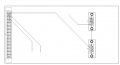
And I am now confused with which side is the top view since there are lines on both sides.
My original thoguht was 1.jpeg from previous messages should be the top vıiew.
the DIN connector on the card itself is 90° tilted tail style just like in the photo attached. So I thought I should use the ANGLE-90 model. But PCB model of this one yields 180° rotated version as you said.
And I am now confused with which side is the top view since there are lines on both sides.
My original thoguht was 1.jpeg from previous messages should be the top vıiew.
On the picture you supplied it is facing to the right. I think it should face to the left. rotate it by 180 degree and think about the view you are using. It is not clear if the view you provide is from the component side or from the bottom. Also it could be that you
unintentionally moved your DIN connector to the wrong side of your PCB. Maybe provide us with a screenshot of your PCB editor with the PCB.
Hi,
- Is there a reason you used a DIN connector with 3 rows instead of 2? Also you changed the same connector to a non 90° one. This changes the mouting holes on the side of the connector, as far as I know.
- Also the D-Sub9 connectors aren't 90° ones.
- The thick copper area is missing.
- The board outline is bigger than in the original design.
- How thick are your connections? They look very thin.
 Facebook
 Google
 GitHub
 Linkedin