Before you leap into phase shift oscilators, and darlington configs. and bootstrapping,
It is apparent from the schem. in this post, you are stumbling on getting a transistor biased into its linear region.
Follow these steps to see how this schem. is not designed properly.
First you have 10v. supply.
[(V1 x R2) / (R1 + R2)] = 4.44v. equals base voltage.
Now subtracting Vbe of 0.65v. from this base voltage , you now have around 3.8v., this is the voltage across the resistor labled R4, which is 500 ohms.
Now the current through R4 is (3.8v. / 500 ohms) = 7.6mA.
For first order aproximation, assume that current value to be the current that will also flow through R3, which will produce a voltage drop of, (7.6mA. x 2K ohms) = 15.2v.
You are only using a 10v. supply, so it is impossible to use these resistor values.
If you want a basic approach to this design here is a way to do it.
Kepping your 10v. and using the value of 7mA. for collector current.
Since you are biasing this into its linear region, then use this rule of thumb.
Make the voltage drop 1/2 of the supply voltage, across the collector resistor. So design this with 5v. across R3.
therefor R3 will = (5v. / 7mA.) =~ 680 ohms.
Now to solve for the emitter resistor R4, design this to have 1V. drop across the transistor itself.
That means the voltage that is left will be across R4.
Voltage across R4 = (10v.VCC - 5v.R3 - 1v.transistor) = 4v. left over to be across R4. which is called "VE"
Now with 4v. across R4, VE, you can solve the value for R4, by using this equation, R4 = (VE / IC), where IC was established in the beginning of this excersise to be 7mA.
So R4 = (4v. VE / 7mA. IC) =~ 560 ohms.
Now for this to work, you have to establish the voltage divider resistors that will put a voltaqge at the base to cause the transistor to be turned on, here is how it is done.
Base voltage (VB) = emitter voltage (VE) plus Vbe (0.65v.)
given as VB = (VE + 0.65v.) = 4.65v. which will be applied to the base of this transistor, to make it turn on, and produce close to the current value of 7mA. that this is being designed for.
To solve for the resistors needed to make this happen, you need to use some more equations.
First make R2 to be around 10 times greater than R4.
So R2 will equal 560 ohms times 10, which would be 5.6K ohms.
Now to solve for R1 use these two equations.
Solve for divider current, first, by taking this equation here.
(divider current (ID), equals , base voltage (VB) divided by R2.
given as ID = (VB / R2) = (4.65v. / 5.6K ohms) = 830uA.
Now R1 can be solved by using this additional equation,
R1 = [(VCC - VB) / ID] = [(10v. - 4.65v.) / 830uA.] =~ 6.2K ohms.
Now build this circuit on your computer and check the voltages with respect to ground, at the collector and the emitter and the base, and see if they are close to the calculated values in this excersise.
Once you do that, THEN, follow the same procedure outlined, BUT THIS time make the voltage drop across the transistor to be 2.5v. and solve for the values of the resistors R4, R2, and R1. in that order.
And again simulate it and check the voltages as you did before, then as a final excersise use 2.5v. across the transistor again, but THIS TIME make the collector current (IC) be 10mA instead of the 7mA, you were using, and solve for the resistors R3, R4, R2, and R1 in that order.
Using the same techniques as given above.
Then let us know how you did, post your results for us to evaluate how you did on this.
Then we can show you how to modify these circuits to get voltage gains so it would act as an amplifier.
Hello Hobbiest,
The circuit is a darlington emitter-follower. It does not have a collector resistor.
The darlington is supposed to be bootstrapped to increase its AC input impedance.
But the circuit is drawn wrong and each part has two part numbers.
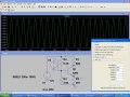
Your signal generator is shorting the base of the transistor to +1V (its offset voltage) in the first schematic and is shorting the base to 0V in the second schematic.
Add an input coupling capacitor so the signal generator does not affect the base bias voltage for the transistor. Then you will see that the transistor is biased wrong so it is almost saturated.
You do not show where the output is from. You should point to the collector.
In the first schematic, do you know why the voltage gain is less than 2?
I am not a SIR!
Your signal generator is a DC dead short at the input of your transistor which causes R3 and R4 to be useless. The first schematic has a +1V offset voltage on your signal generator so the base of the transistor is at +1.0VDC. Then the emitter is at about +0.3DC and the collector is at about 11.55VDC which is nearly cutoff.
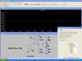
The second schematic has no offset voltage on the signal generator so it shorts the base of the transistor to 0VDC and then the transistor has no output (it is completely cutoff at +12VDC).
If you add an input coupling capacitor then R3 and R4 set the base of the transistor at
+4.2V, the emitter will be at about +3.5V and the collector will be at about +4.8V which is nearly saturated.
what value of capacitor should be used for coupling??
Select the lowest frequency you need at almost full output level. Then learn about the reactance of a capacitor at that frequency. It is an important and simple formula. Ask your teacher.
The capacitor feeds R3, R4 and the input resistance of the transistor all in parallel. Then the lower frequencies have their level reduced.
I already told you that if you add an input coupling capacitor then R3 and R4 bias the transistor wrong so it is almost saturated. R3 and R4 should set the base voltage a little lower which will cause the emitter voltage to be lower and the collector voltage to be higher then the collector can swing more.
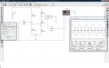
I drew up your circuit and simulated it in multi.sim.
I used very large capacitors, for input and output, 1000uF.
These coupling capacitors is used to transfer the AC signal in and out of the stage while keeping all DC (biasing) voltages from being hindered from the input and output devices.
The input signal must be very small, for this type transistor, this is a general purpose small signal amp, (transistor 2n3904).
So if after you simulate your circuit, and find there is distortion on the output signal, then continue to lower the input voltage until distortion dissapears.
There are reasons this happens, that get into more technical details, which you will learn as you continue your education.
You have around 5v. at the collector, which is close to the 1/2 supply value, this is what the simulator shows.
Now as audioguru said,
Do you know why the small gain with this stage.
It is due to the ratio of ( R1 / R2), which is close to around double the input signal.
To get more voltage across the transistor you would need to lower the value of R2, that will also increase the voltage gain, (R1 / R2),
however at this cost it will also lower the input impedance, so there is always a tossup between input impedance and gain of a stage.
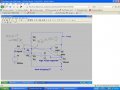
Here is the results of your design simulated:
Input signal is red, and the output is blue on the Oscope.
Draw this the same way in your simulaor, and then practice biasing it and amplifying signals.
Youll get it, just keep working at it, and ask the forum questions as needed.
Ok, i want to know on changing the offset voltage the output waveform changes, why??,
why you have connected large bypass capacitor, how it is calculated??
and why you have said to take voltage across transistor (i.e.) 2.5V??
There is no "bypass capacitor". Hobbiest added an input coupling capacitor and an output coupling capacitor to pass the AC signal but block DC. His 1000uF is much too much capacitance. The formula is C= 1 divided by 2 pi Rf where R is R3, R4 and the input resistance of the transistor in parallel and f is the frequency that is at -3dB.
why you have said to take voltage across transistor (i.e.) 2.5V??
The transistor should be biased so that its output can swing an equal amount in a positive direction and in a negative direction. But you had the collector DC voltage too low so the transistor was almost saturated. You can increase the collector voltage by increasing the value of R4.
From my course material, I pretty much learned the importance of calculating the bypass capacitors, for a cutoff frequency, and have learned through experiance that putting a bypass capacitor too large with respect to calculated value, can upset the stability of the stage, due to too much overall gain, ect...
We also learned the importance of using break frequencies, when coupling more than 2 stages, to keep from oscillating, but personally when I built my circuits in the past, before I joined this forum, years way back, I had the assumption, that as long as a coupling capacitor, was large enough to pass the lowest frequency needed, than the larger the better.
However there seems to be a lot of emphasis, given to the students that come on this board, from there college professors, to not only calculate the value of the bypass capacitors, but also to calculate the coupling capacitors too.
My old addage, the larger the better, is really making me question, now, especially since you posted that the large capacitor I used was way too large, (1000uF), I'm beginning to see that maybe there is a limit too how large to make the coupling network, Not only cost effectiveness, but performance wise.
So am I correct to say than that using coupling capacitors close to calculated values within tolerance, does significantly help the perfornmance of the transistor stages, especially to keep them from oscillations?
Because essentially, the coupling capacitors in series with the input resistances, are filters, and RC filters are sesigned to work using cutoff frequencies, in the equation, so is it best to treat the coupling network as if you were designing a RC highpass filter.
I do not intend to hijack this thread, just wanted to ask this question. While this thread is on this subject.
Hi Hobbiest,
Your huge input coupling capacitor (not a bypass capacitor that stops oscillations) takes "weeks" to charge. Until it is charged then the transistor will produce severe distortion. A few uF will work fine for audio frequencies and will charge in a fraction of a second.
Yes, it is a highpass filter.

 Facebook
 Google
 GitHub
 Linkedin


 122.2 KB Views: 24