Facebook
 Google
 GitHub
 Linkedin

Hi everyone, I’m new to this community, so please bear with me. I hope this is the right place for this kind of troubleshooting request.
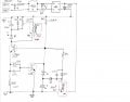
I’m trying to repair an old Daikin outdoor unit controller board. I don’t have the schematic, so I’m reverse‑engineering the circuit on the bench.
So far I have found two failed components:
I replaced both with new parts, but they failed immediately on power‑up. For safety, I also replaced the bridge rectifier and the main electrolytic capacitor (C9). Now I’m trying to identify what is causing the repeated failure.
I would also like to replace C13 and the Zener diode, but the Zener marking is unreadable.
Some components were tested in‑circuit because the board is double‑sided with plated‑through holes, and removing parts risks damaging the PCB.
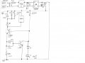
At this point I’m looking for help analyzing the part of the circuit shown in my draft (attached). Please note that some small components may be missing from the drawing.
My main questions are:
The capacitor shows visible cracks on the sides, so I suspect it may be faulty.
Any help understanding this section of the circuit or confirming the likely failing component would be greatly appreciated.
I found a very similar circuit here in this form in an old thread: https://forum.allaboutcircuits.com/threads/is-this-a-class-c-amplifier.132927/ posted by @Jony130 ...maybe you have some ideas?
Thanks in advance for your help!!!
fuzzy logic
I’m trying to repair an old Daikin outdoor unit controller board. I don’t have the schematic, so I’m reverse‑engineering the circuit on the bench.
So far I have found two failed components:
- R5 (5 Ω / 5 W)
- 2SC3751 transistor (it is the switching transistor driving the flyback transformer (trafo) primary)
I replaced both with new parts, but they failed immediately on power‑up. For safety, I also replaced the bridge rectifier and the main electrolytic capacitor (C9). Now I’m trying to identify what is causing the repeated failure.
I would also like to replace C13 and the Zener diode, but the Zener marking is unreadable.
Some components were tested in‑circuit because the board is double‑sided with plated‑through holes, and removing parts risks damaging the PCB.
- D1 seems fine (tested with a multimeter).
- The resistors in the area measure correctly, as shown in my draft schematic.
- I also removed and tested the C1815 transistor, which appears to be OK (I'll replace with a new one)
At this point I’m looking for help analyzing the part of the circuit shown in my draft (attached). Please note that some small components may be missing from the drawing.
My main questions are:
- What could be causing the repeated failure of the 2SC3751?
- Is there a typical Zener value used in this kind of base‑drive network?
- Could C13 (the capacitor in the snubber/clamp network across the primary) cause this failure if it is open or degraded?
The capacitor shows visible cracks on the sides, so I suspect it may be faulty.
Any help understanding this section of the circuit or confirming the likely failing component would be greatly appreciated.
I found a very similar circuit here in this form in an old thread: https://forum.allaboutcircuits.com/threads/is-this-a-class-c-amplifier.132927/ posted by @Jony130 ...maybe you have some ideas?
Thanks in advance for your help!!!
fuzzy logic