TRANSIMPEDANCE AMP FOR 5nA Signal

Thread Starter

longpole001

Joined Sep 16, 2014
62
Hi guys , i have a need which calls for a photodiode receiving very small signal in 5nA peek current , at about 3uS pulse rate , for bursts of about 100hz . the output would need to drive a A/D on PIC so a 2nd stage amp 100mV peek would be required .

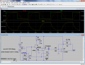
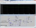
I have been looking at many TIA designs and the Photodiode i need has 50pf with about 12v bios applied ,

i was trolling through the site and came across a suggested design . which looks like it may be applied but since i am new to TIA designs and such a low signal value to get from a Photodiode , need some guidance in the TIA and 2nd stage design to get this signal .

http://forum.allaboutcircuits.com/attachments/photodiode-interface-jpg.38952/

Regards

Sheldon
 

Thread Starter

longpole001

Joined Sep 16, 2014
62
i have several i am considering but given the very low signal level and limited space for additional optics , a large active area is prefered ,

to counter the higher capacitance negative bios is likely to need be applied ,

best one i like so far is S6801-01 , as it has the bandpass filter and a built in lens , and can get down to about 50pf with 10v RV applied , but all have pros and cons for this signal detection

love an APD , but thats not real cost option

http://www.osram-os.com/Graphics/XP..., Lead (Pb) Free Product - RoHS Compliant.pdf

http://www.hamamatsu.com/jp/en/product/category/3100/4001/4103/S6775-01/index.html

http://www.hamamatsu.com/jp/en/product/category/3100/4001/4103/S6801-01/index.html

http://www.thorlabs.hk/thorproduct.cfm?partnumber=FDS100
 

Thread Starter

longpole001

Joined Sep 16, 2014
62
mmm that does look worth a try , i am waiting on the photodiode of my choice , but i have a few with a 1 mm active area , for test on sensitivity of the TIA

this also caught my eye , as i like the Jfet front end and the lower cost op amp at the output with a good size signal swing , it may suit
http://www.linear.com/solutions/1785

found this as well
http://www.analog.com/designtools/en/photodiode/#/circuitDesign , which looks nice
http://www.analog.com/designtools/en/photodiode/Share?id=949

i think noise is going to be areal concern as with this application , i endup puting in 20mv output , on 3us time , using 12v BV , 50pf , on 4.65nA , to see with a low Q value , tool recommend ad8616 , with a 2nd stage

i know it not 100mV output but i think i can use the quad version of the chip to take it to the next stage of upto larger 100-500mv per pulse for the A/D on the pic

what your thoughts

cheers

sheldon
 

Thread Starter

longpole001

Joined Sep 16, 2014
62
ok thanks , it seems that tool link does not have the AD8627 range in the selection option , which i am sure they will fix

even with best amp it seems ill need to optically amplify this signal a fair 4/1 or more before any amp can make good uses of it without the large amount of noise which is sure to be there
 

Thread Starter

longpole001

Joined Sep 16, 2014
62
"Although the LT1028/LT1128 input stage operates at nearly 1mA of collector current to achieve low voltage noise, input bias current is only 25nA."
I am wondering if the Jfet reduces the bias current for my very small 5na enough without a lot of noise and signal loss ??????
 

Thread Starter

longpole001

Joined Sep 16, 2014
62
rephase - would the input from the photodiode at 5na be enough to make the jfet conduct to allow the 25na input bios for the amp ?
 

Thread Starter

longpole001

Joined Sep 16, 2014
62
ok ill give it a try
from the simulations using the tool as base , best i get is about 10-25mV for peek signal of 5nA and about 1.5nA min signal / noise , and will require a further 1 or 2 stages for a signal of about 500mv - 1V , but the noise is likely to be a problem
 

ronv

Joined Nov 12, 2008
3,770
For sure some more input would really help.
Here is what I have for 100mv output.
Some things to think about.... The circuit has some DC offset. I don't know what you are doing so don't know if that is a problem or not.
It is also sensitive to noise on the 15 volt line so for sure this should be a linear power supply.
Because of the high speed op amps it would just as soon oscillate as amplify so you will need to be careful with the layout.
 

Attachments

Thread Starter

longpole001

Joined Sep 16, 2014
62
thanks for that , yes layout is going to be a big factor in the noise , even when i am breadboard just to see the general response , and its so easy to osc
the dc offset will be part of the problem as well , which will need to be allowed for
 

MrChips

Joined Oct 2, 2009
34,896
Layout is critical. Use SMT components, solid ground plane on the bottom layer, 0.1uF decoupling capacitors right at the power and ground pins, and a guard ring around the inputs of the opamp (that is, the AD8067).
 
Last edited:

Thread Starter

longpole001

Joined Sep 16, 2014
62
wow , thats very interesting , it appear that the additional cap of the diode is allowing the jfet input stage to be behave with a larger swing , a lot more than i would have expected
 

ronv

Joined Nov 12, 2008
3,770
The output is still the same. V=IpdX1meg. But the signal is cleaner. Would you get more current from the larger diode for the same amount of light?
 
Top