Transimpedance circuit with phototransistor

Thread Starter

leboschmit

Joined Apr 2, 2025
4
Hello,

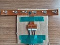
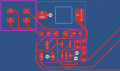
I am currently facing a problem: the schematic you see works on a bread board but the pcb layout gives me constant analog values an the STM32 ADC is nearly fixed.

1746383814189.png

1746383957562.png

I am thankful for any help.
 

schmitt trigger

Joined Jul 12, 2010
2,031
When you say: it gives me constant analog values; what are those values?
And have you attempted to read the actual opamp output with a DMM?

EDIT: looking closely, the board artwork DOES NOT represent the schematic.
If you require help, show the actual schematic of the board artwork.

EDIT2: Show the silkscreen with the corresponding reference designators.
 
Last edited:

WBahn

Joined Mar 31, 2012
32,707
You might start with verifying your part number and the corresponding pinout:

1746390988944.png

Your layout is using Pin 1 as the output.

But your schematic indicates you are using the DCK package, which has the output on Pin 4.

Beyond that, if you want people to troubleshoot your layout, make it as easy for them as possible.

Give every net a decent name and be sure that those names are on both the schematic and the layout. If you don't want to assign good names, then at least annotate the schematic with the names that are autogenerated and shown in the layout. Then, don't just put 'R' or 'C' on the layout, make it clear WHICH schematic component is being referred to by using the reference designator, so 'R16' or 'C9'.

Also, provide more meaningful information about what you are seeing versus what you expect. Saying that something gives you nearly constant analog values doesn't say much. What values are you seeing? What do you expect to see? What does it mean for STM32 ADC to be nearly fixed? Your schematic doesn't have an STM32 anywhere in it, so how can anyone possibly know what you mean by it being "nearly fixed", let along how it relates to the schematic and/or layout you've shown?
 

Thread Starter

leboschmit

Joined Apr 2, 2025
4
Thank you WBahn, I actually had the wrong footprint in my design!

I fixed that and assembled a new PCB. Now, I am facing strange behaviour, that occours on all 6 ADC inputs.

For my next layout I will use your help and tips for later troubleshooting.
For now, I try my best to explain my design:

I have the following behaviour:
https://youtube.com/shorts/HwivlzGKf6A

1. All ADCs read "mainly" between 0 und 720
2. Sometimes it jumps up to 4030
3. There also seems to be some noise, which is sporadic

I apologise for my bad documentation. If there is any way, I can provide better data to get help, please let me know!
 

Attachments

Thread Starter

leboschmit

Joined Apr 2, 2025
4
Thank you WBahn, I actually had the wrong footprint in my design!

I fixed that and assembled a new PCB. Now, I am facing strange behaviour, that occours on all 6 ADC inputs.

For my next layout I will use your help and tips for later troubleshooting.
For now, I try my best to explain my design:

I have the following behaviour:
https://youtube.com/shorts/HwivlzGKf6A

1. All ADCs read "mainly" between 0 und 720
2. Sometimes it jumps up to 4030
3. There also seems to be some noise, which is sporadic

I apologise for my bad documentation. If there is any way, I can provide better data to get help, please let me know!

Edit: I think I accidently switched the inverted input of my OPA391 with the GND. Pin 2 and 3 are switched.
 
Top